
Gray scale x-ray mask

a mask and x-ray technology, applied in the field of lithographic masks, can solve the problems of difficult handling and fragile masks

Inactive Publication Date: 2006-03-07
NAT TECH & ENG SOLUTIONS OF SANDIA LLC
View PDF4 Cites 10 Cited by
  • Summary
  • Abstract
  • Description
  • Claims
  • Application Information

AI Technical Summary

Benefits of technology

[0011]What is needed is a simple method for providing microstructures that smoothly vary in height from point-to-point in etched substrates, i.e., structure which can vary in all three dimensions. Also needed is a simple, so-called “gray-scale” mask wherein the mask structures have variable attenuating properties from point-to-point across the mask surface. Such a mask could be used to provide etched features in silicon having arbitrary three dimensional shapes which could themselves be used as a final device or as a plating base for providing a metal embossing stamp.
[0015]Yet another object of this invention is to provide a simple method for fabricating a gray scale mask useful for ultraviolet and for x-ray radiation.

Problems solved by technology

Such masks are, however, quite fragile and difficult to handle.

Method used


Image

  • Gray scale x-ray mask
  • Gray scale x-ray mask
  • Gray scale x-ray mask

Examples

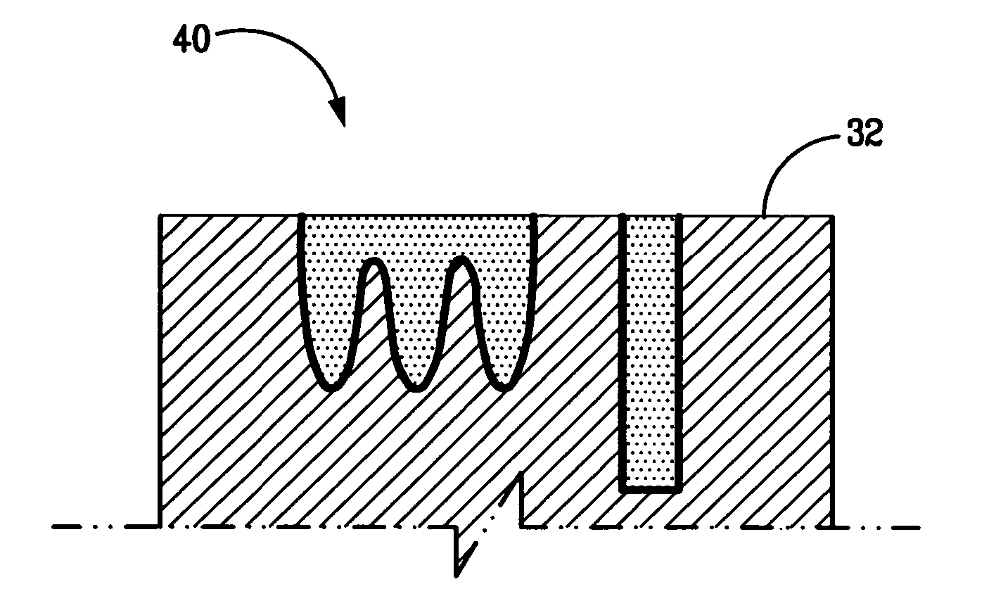
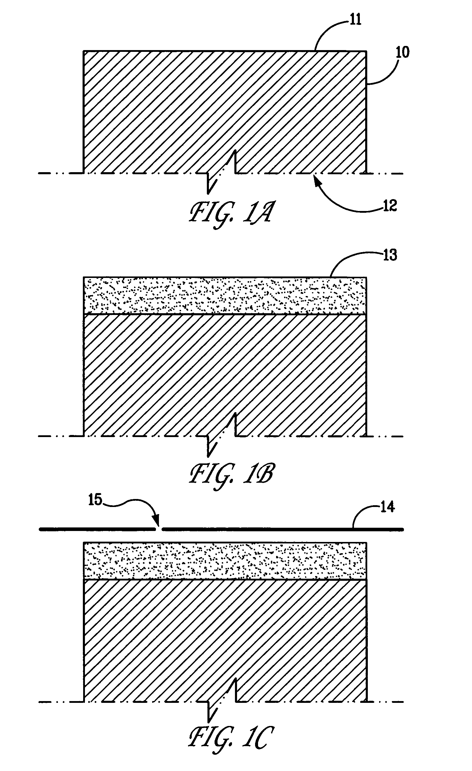
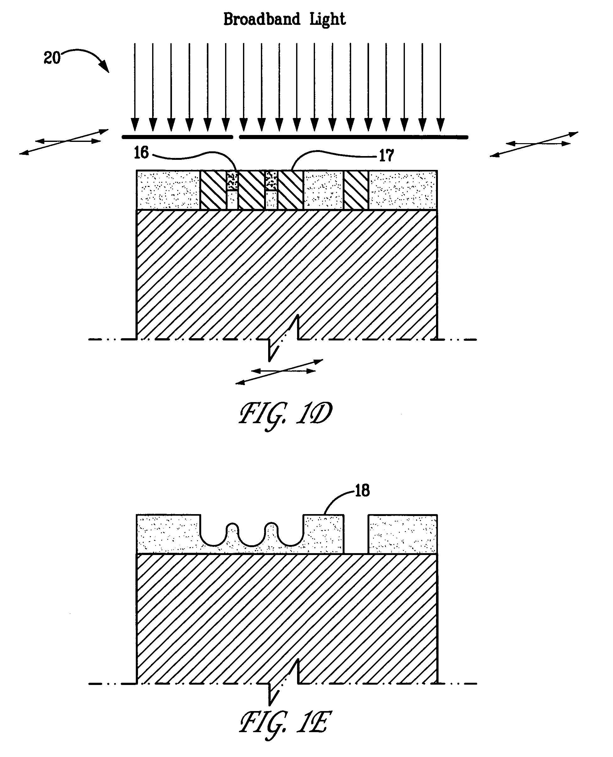

Embodiment Construction

[0027]The present invention describes a process for fabricating three dimensional imprint tools. Also described is a gray-scale mask for replicating the image of these three dimensional tools.

[0028]In order to achieve these and the other objects of the invention a process is described wherein an image is transferred into a photoresist material in such a manner as to create an exposure gradient across those portions of the resist exposed to radiation. The process otherwise teaches using known lithographic techniques to expose a pattern into a thin layer of photoresist applied to a silicon substrate. The exposed image is developed to remove a portion of the photoresist (positive resists) from the surface of the silicon, and the substrate etched by a reactive plasma technique in those regions free of the resist in order to provide a series of trenches on the silicon surface. (It should be noted that because negative resists react to light exposure by cross-linking the polymer comprisin...


PUM

PropertyMeasurementUnit
thickaaaaaaaaaa
etch depthaaaaaaaaaa
thicknessaaaaaaaaaa

Abstract

The present invention describes a method for fabricating an embossing tool or an x-ray mask tool, providing microstructures that smoothly vary in height from point-to-point in etched substrates, i.e., structure which can vary in all three dimensions. The process uses a lithographic technique to transfer an image pattern in the surface of a silicon wafer by exposing and developing the resist and then etching the silicon substrate. Importantly, the photoresist is variably exposed so that when developed some of the resist layer remains. The remaining undeveloped resist acts as an etchant barrier to the reactive plasma used to etch the silicon substrate and therefore provides the ability etch structures of variable depths.

Description

CROSS REFERENCE TO RELATED APPLICATIONS[0001]This application is a divisional application prior U.S. patent application Ser. No. 10 / 146,421 originally filed May 14, 2002 now U.S. Pat. No. 6,749,997.STATEMENT OF GOVERNMENT INTEREST[0002]The United States Government has rights in this invention pursuant to Contract No. DE-AC04-94AL85000 between the United States Department of Energy and Sandia Corporation, for the operation of the Sandia National Laboratories.BACKGROUND OF THE INVENTION[0003]1. Field of the Invention[0004]The present invention relates to a lithographic mask capable of providing regions of graded exposure, such that when combined with anisotropic etching provides three dimensional microstructures of arbitrary size and shape (generally non-prismatic). The present invention also relates to a method for producing a gray-scale x-ray mask and fabricating a tool useful in the preparation of plated molds, or embossing stamps, for printing fine structures into plastic substrat...

Claims


Application Information

Patent Timeline
Patent Type & Authority Patents(United States)
IPC IPC(8): G03F7/20G03F9/00B29C33/38B29C33/42G03F1/00G03F1/22G03F7/00
CPCB29C33/38B29C33/424G03F1/144G03F1/22G03F7/0017G03F7/203Y10T428/12361Y10S430/167Y10T428/12743Y10T428/12778Y10T428/12708Y10T428/12486G03F1/50
Inventor MORALES, ALFREDO M.GONZALES, MARCELA
Owner NAT TECH & ENG SOLUTIONS OF SANDIA LLC
Learn More