Particle multibeam lithography

Inactive Publication Date: 2006-01-24
IMS NANOFABTION
View PDF14 Cites 44 Cited by
  • Summary
  • Abstract
  • Description
  • Claims
  • Application Information

AI Technical Summary

Benefits of technology

[0013]According to the invention, it is possible to implement the basic focusing properties independent of the adjustment of the individual image of the sub-beams, Thus, the invention provides a simple solution for the treatment of the imaging aberrations and the positioning of the individual sub-beams independently of each other. Due to the very accurate positioning of the beams on the substrate to be structured, the use of a deflection unit allows a relaxed requirement on the accuracy for the mechanical positioning of the wafer stage. This reduces the production expenditures and simplifies adjustment of the components of the lithography setup as well as controlling during operation The apertures defining the sub-beams are separated from the extraction system. This appreciable circumstance results in an augmented tolerance with respect to deviations in the extraction geometry as well as in the position of the apertures with respect to the sub-beam axes.
[0024]Moreover, it simplifies production and operation of the lithographic device if several aperture plates are provided which are penetrated by the sub-beams, said aperture plates having openings forming aperture lenses having a focusing effect on the sub-beams.

Problems solved by technology

Moreover, the reduced particle density results in a distinctly lowered influence of the Coulomb interaction within each sub-beam and thus in a smaller contribution to imaging aberrations.
In J. J. Muray's multibeam device design, however, the aperture screen is positioned in proximity to the wafer, which gives rise to problems such as contamination of the screen apertures by substances produced in the course of the processing of the substrate.
Moreover, an individual adjustment of the sub-beams cannot be realized due to the restricted space situation.
For these reasons, this design was not considered suitable for commercial lithography purposes.
The adjustment of the imaging properties and correction of imaging aberrations via the individual objective lenses, though not treated explicitly in the article of N. Shimazu et al., is difficult because of the very restricted conditions of space in the target region.
Moreover, often the close position of the objective lenses to the substrate will bring about problems arising from the byproducts of the substrate treatment, for instance with the well-known outgassing of resist layers.
It should be noted, however, that whenever a set of sources is required, in particular one source for each of the beams to be used, this complicates the implementation of a multibeam setup and, moreover, it is difficult to maintain a sufficiently homogeneous set of beams.
Moreover, since each individual miniature column comprises a complete equipment of an electron microscope, the implementation of a multibeam lithography system requires great expenditures during production and maintenance, and in particular during adjustment of the miniature columns. Q. Ji et al., in the article “A New Focused Ion Bean System for Maskless Direct-write Lithography” of the conference proceedings of the '43rd International Conference on Electron, Ion and Photon Beam Technology and Nanofabrication' (EIPBN '99), Marco Island, Fla., Jun. 1-4, 1999 (to be published in J. Vac. Sci. Technol.
The magnetic field used for focusing has to be very homogeneous; the provision of individual adjustment of the magnetic focusing of the individual beams would be very complex.
In order to provide for a way of individual adjustment of the beams, arid also in order to compensate for the small depth of focus of the magnetic focusing system, fine correction elements using electric fields are required, and thus the total magneto-optical imaging system becomes intricate and difficult to realize.
Due to the small size of the beam radius, namely about 1 μm (or even less), this setup requires a considerable current density, which cannot be achieved reliably in a demountable vacuum setup such as a semiconductor production device.
Also, due to the use of photocathodes the Groves and Kendall / Pickard et al. system is restricted to electron beams.
Moreover, it is a well-known disadvantage of photocathodes that they are very susceptible to contaminations and require a UH vacuum.

Method used


Image

  • Particle multibeam lithography
  • Particle multibeam lithography
  • Particle multibeam lithography

Examples


Embodiment Construction

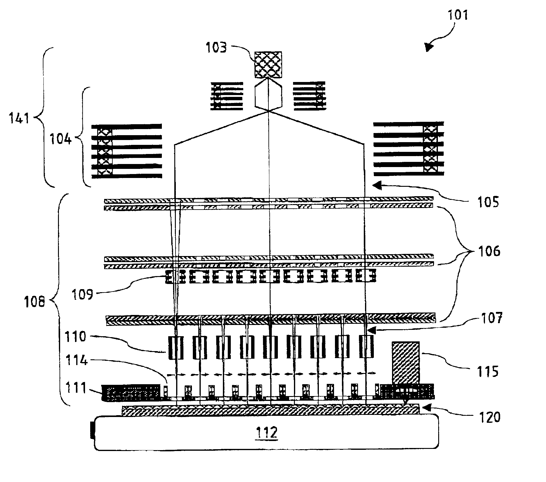
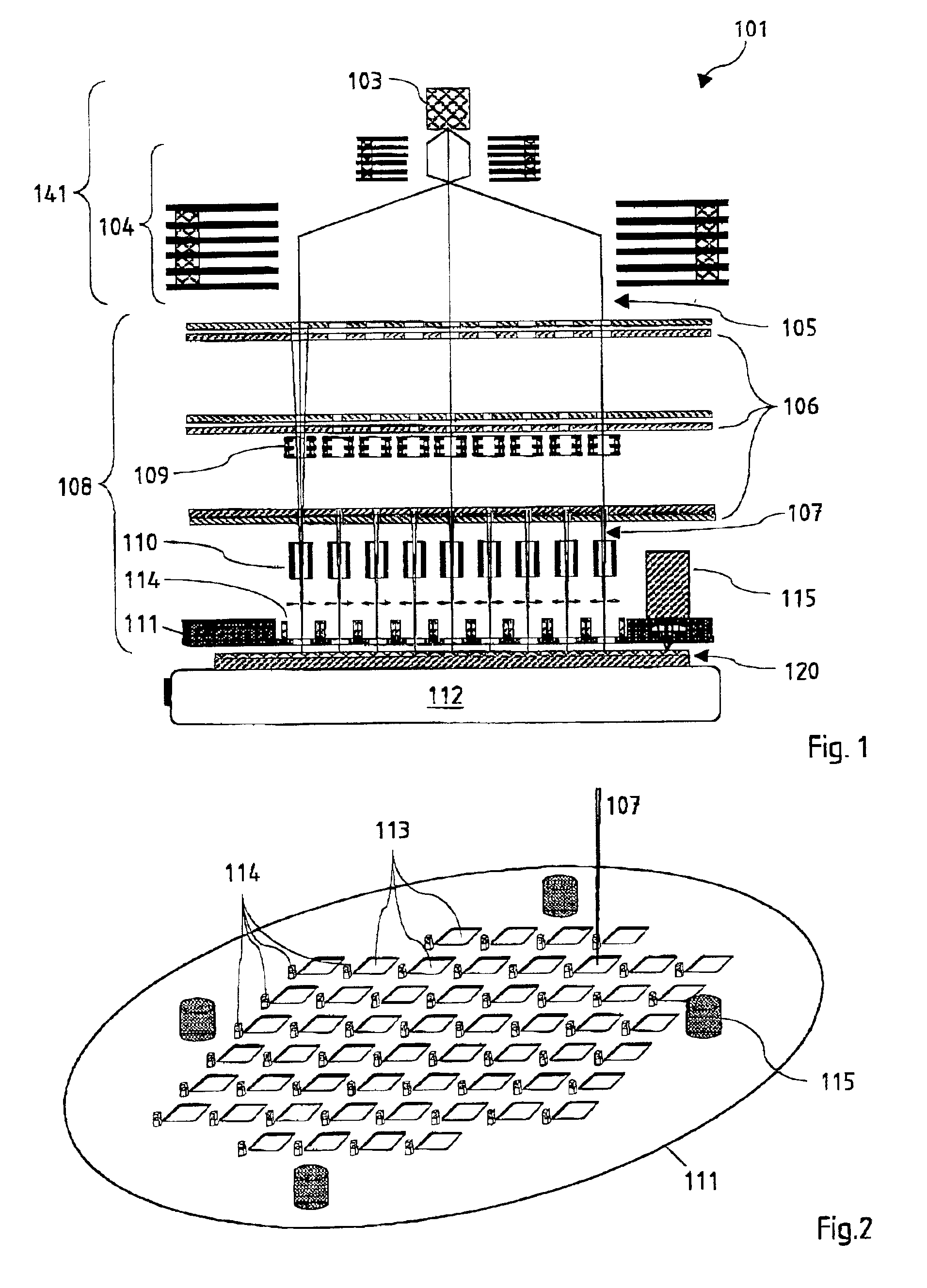
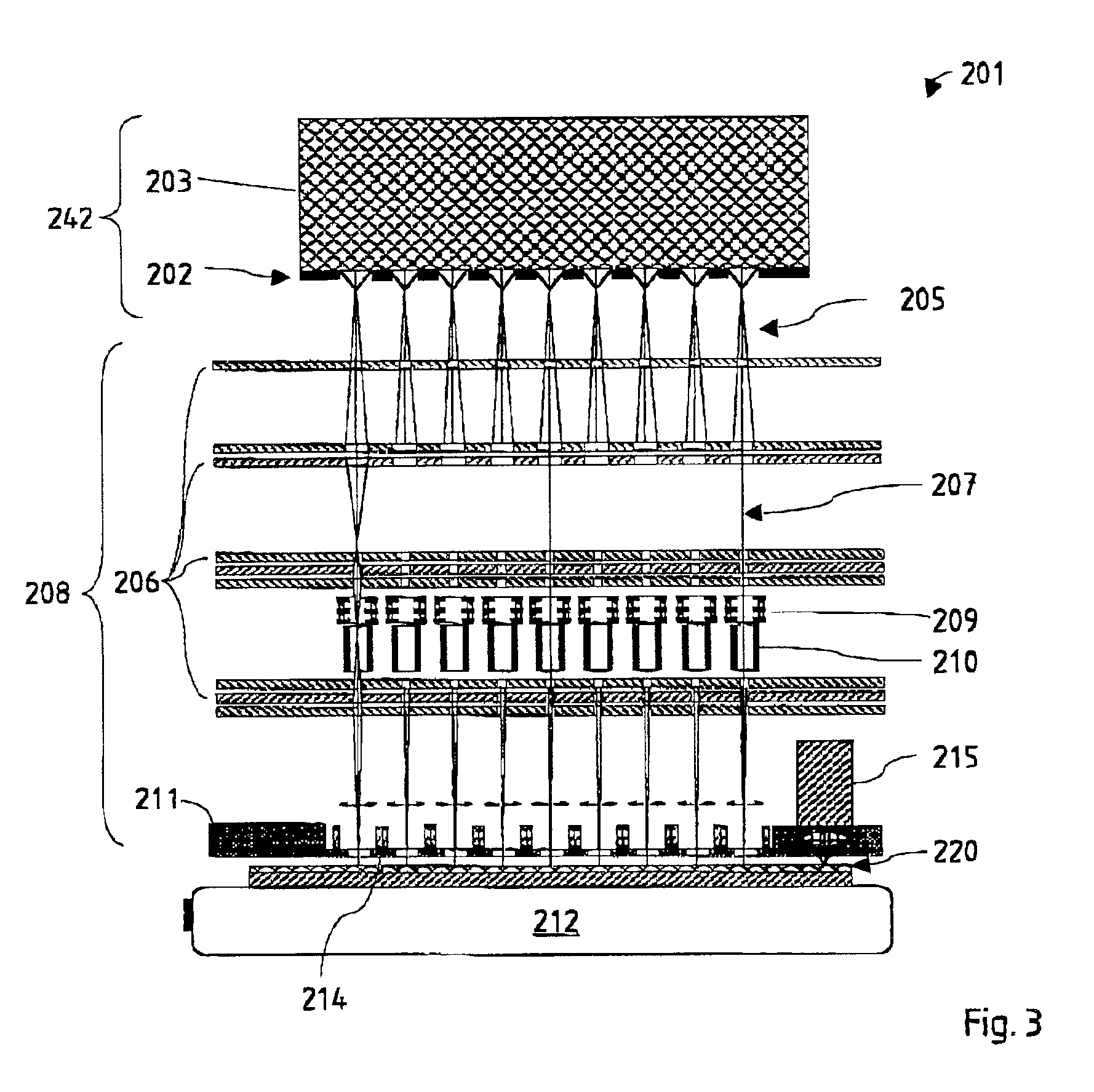
[0038]As a first preferred embodiment of the invention, an exemplary ion multibeam lithography system 101 is shown in the schematic longitudinal section of FIG. 1. This lithography system is arranged for writing of structures onto a resist-covered wafer substrate 120. The first part of the system, the illumination system 141, comprises an ion source 103 and a collimator optics system 104 and serves to produce a broad ion beam 105. The total width of the illuminating beam 105 produced by the illumination system 121 is at least a wafer diameter, e.g., 300 mm. A collimator optics system for producing a particle beam of this kind is disclosed by G. Stengl et al. in the U.S. Pat. No. 5,742,062. The beam 105 is substantially homogeneous over its width so as to have a particle flow sufficiently uniform within the allowed tolerances for all individual beams which are produced from the illuminating beam.

[0039]The illuminating beam 105 emerging from the illuminating system 141, is telecentric...


PUM


Abstract

In a particle multibeam lithography apparatus an illumination system (242) having a particle source (203) produces an illuminating beam (205) of electrically charged particles, and a multibeam optical system (208) positioned after the illumination system (242) and comprising at least one aperture plate having an array of a plurality of apertures to form a plurality of sub-beams focuses the sub-beams onto the surface of a substrate (220), wherein for each sub-beam (207) a deflection unit (210) is positioned within the multibeam optical system and adapted to correct individual imaging aberrations of the respective sub-beam with respect to the desired target position and / or position the sub-beam during a writing process an the substrate surface. Preferably, for each sub-beam the respective aperture of the first aperture plate defines the size and shape of the sub-beam cross-section and the multibeam optical system produces a demagnified image of the aperture on the substrate surface, with a demagnification of at least 20:1.

Description

FIELD OF THE INVENTION AND DESCRIPTION OF PRIOR ART[0001]The invention relates to multibeam lithography by means of electrically charged particles.[0002]More exactly, the invention refers to an apparatus for multibeam lithography by means of electrically charged particles, comprising an illumination system having a particle source, the illumination system producing an illuminating beam of said electrically charged particles, and a multibeam optical system positioned after the illumination system as seen in the direction of the beam, said multibeam optical system comprising at least one aperture plate having an array of a plurality of apertures to form a plurality of sub-beams, wherein the multibeam optical system focuses the sub-beams onto the surface of a substrate.[0003]Likewise, the invention relates to a method for multibeam lithography by means of electrically charged particles, wherein a particle beam is produced by a particle source, transferred into an illuminating beam and ...

Claims


Application Information

Patent Timeline
IPC IPC(8): H01J37/08H01J37/317
CPCB82Y10/00B82Y40/00H01J37/3177H01J37/3174H01J2237/153
Inventor LOSCHNER, HANSSTENGL, GERHARDVONACH, HERBERTPLATZGUMMER, ELMAR
Owner IMS NANOFABTION
Why Eureka
Try Eureka