Method and apparatus for strain-stress sensors and smart skin for aircraft and space vehicles
a strain-stress sensor and smart skin technology, applied in the direction of force measurement, electric/magnetic measurement arrangement, instruments, etc., to achieve the effect of improving the aerodynamic quality
- Summary
- Abstract
- Description
- Claims
- Application Information
AI Technical Summary
Benefits of technology
Problems solved by technology
Method used
Image
Examples
example 1
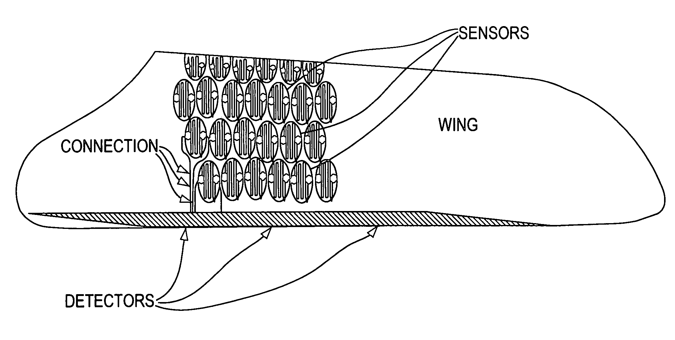
[0045]1. The electrically conducting subject to be coated with smart skin, such as the aircraft wing (as shown on FIGS. 4 and 5) is cleaned with a standard vacuum industry technique.
[0046]2. The subject to be coated with smart skin is located in a vacuum deposition chamber.
[0047]3. Air is pumped out of the deposition chamber up to about 1.0×10⁻⁵ Torr.
[0048]4. The chamber is filled with argon up to a pressure of about 5×10⁻⁵ Torr, and the surface to be coated clean in the argon low pressure discharge for about 10 minutes.
[0049]5. Unalloyed stabilized diamond-like carbon 3 micrometer thick dielectric layer is deposited upon the surface of the structure (FIGS. 4 and 5), such as the aircraft wing using a known technique (see U.S. Pat. Nos. 5,352,493, 5,718,976 and 6,080,470). This unalloyed stabilized diamond-like carbon dielectric layer possesses resistivity in an order of 1012 to 1013 Ohm-cm.
[0050]6. A Chromium-alloyed diamond-like Me—C 0.5 to 1.0 micrometer thick conducting stress se...
example 2
[0068]1. The electrically conducting subject to be coated with smart skin, such as the aircraft wing (as shown on FIGS. 4 and 5), is cleaned with a standard technique of vacuum industry.
[0069]2. The subject to be coated with smart skin is located in vacuum deposition chamber.
[0070]3. Air is pumped out of the deposition chamber up to about 1 0.0×10⁻⁵ Torr. 4. 4. The chamber is filled with argon up to pressure of about 5×10⁻⁵ Torr, and the surface to be coated cleaned in the argon low pressure discharge for about 10 minutes.
[0071]5. Unalloyed stabilized diamond-like carbon 3 micrometer thick dielectric layer deposited upon the surface of the structure (FIGS. 4 and 5), such as the aircraft wing using a known from prior techniques. The unalloyed stabilized diamond-like carbon dielectric layer possesses resistivity in an order of 1012 to 1013 Ohm-cm.
[0072]6. Chromium-alloyed diamond-like Me—C 0.5 to 1.0 micrometer thick conducting stress sensing layer (as shown in cross-section on FIG. 5...
PUM
| Property | Measurement | Unit |
|---|---|---|
| temperature | aaaaa | aaaaa |
| temperature | aaaaa | aaaaa |
| temperature | aaaaa | aaaaa |
Abstract
Description
Claims
Application Information
 - R&D
- Intellectual Property
- Life Sciences
- Materials
- Tech Scout
- Unparalleled Data Quality
- Higher Quality Content
- 60% Fewer Hallucinations
Browse by: Latest US Patents, China's latest patents, Technical Efficacy Thesaurus, Application Domain, Technology Topic, Popular Technical Reports.
© 2025 PatSnap. All rights reserved.Legal|Privacy policy|Modern Slavery Act Transparency Statement|Sitemap|About US| Contact US: help@patsnap.com


