
Interfacial oxidation process for high-k gate dielectric process integration

a dielectric process and interfacial oxidation technology, applied in the field of semiconductor processing, can solve the problems of imposing scaling constraints on the gate dielectric material, the overall dielectric constant of the microstructure, and the need to thin the oxide interfacial layer,

Active Publication Date: 2005-12-13
IBM CORP +1
View PDF13 Cites 21 Cited by
  • Summary
  • Abstract
  • Description
  • Claims
  • Application Information

AI Technical Summary

Benefits of technology

The patent describes a method for making microstructures with an interfacial oxide layer using a diffusion filter layer to control the oxidation of a substrate. This method allows for better control over the growth of the oxide layer and can improve the performance of the microstructures.

Problems solved by technology

The downscaling of CMOS devices imposes scaling constraints on the gate dielectric material.
However, the presence of an oxide interfacial layer lowers the overall dielectric constant of the microstructure and, therefore, the oxide interfacial layer may need to be thin.

Method used


Image

  • Interfacial oxidation process for high-k gate dielectric process integration
  • Interfacial oxidation process for high-k gate dielectric process integration
  • Interfacial oxidation process for high-k gate dielectric process integration

Examples


Embodiment Construction

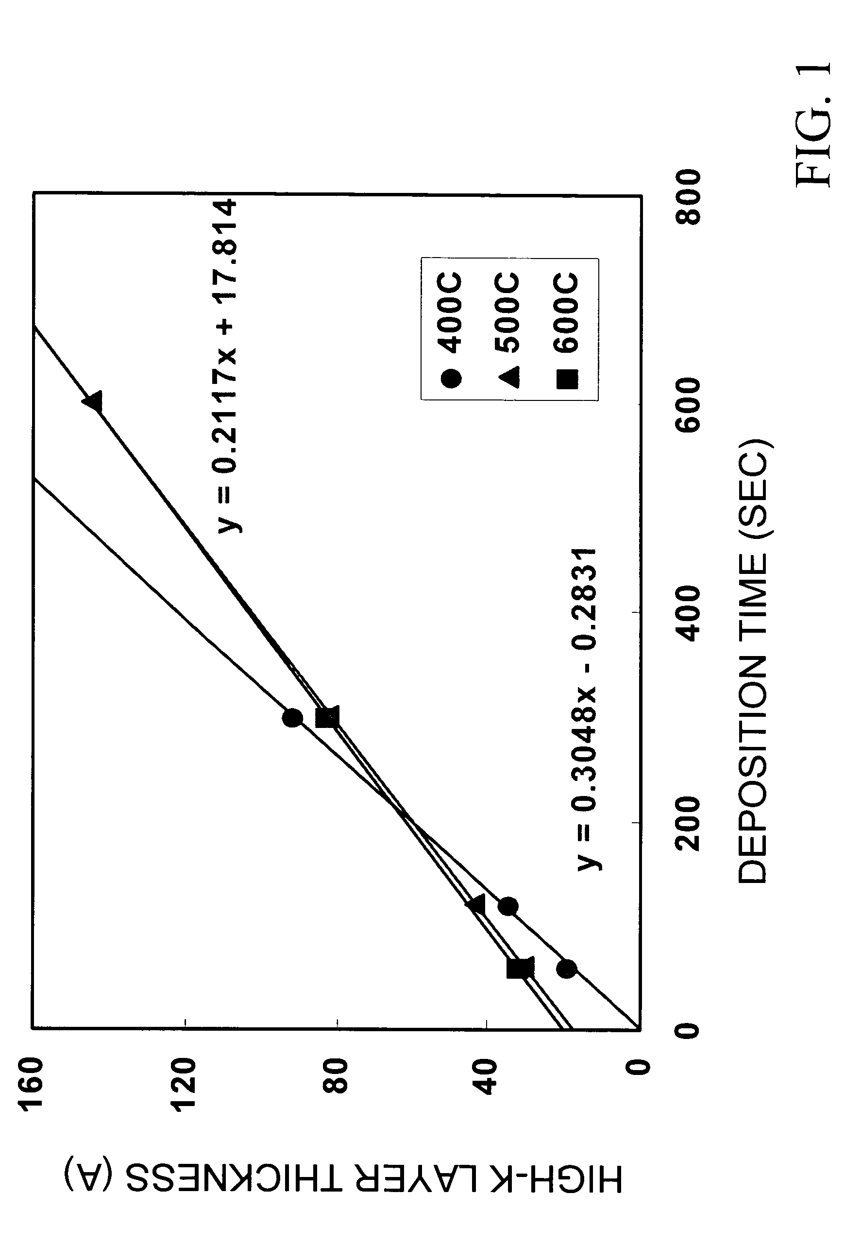
[0020]FIG. 1 shows the thickness of a high-k layer deposited by a TCVD process on a Si substrate as a function of deposition time. A thin native oxide layer was removed from the Si substrate by a wet cleaning process using HF, prior to depositing a high-k layer on the Si substrate. A HfO2 high-k layer was deposited on the clean Si substrate at substrate temperatures of 400° C., 500° C., and 600° C. The HfO2 layer was deposited by a TCVD process utilizing a process gas comprising a Hf(OBut)4 precursor.

[0021]In FIG. 1, the thickness of the HfO2 high-k layers as a function of deposition time was fitted using linear fits of the data points. The linear relationship between the high-k layer thickness and the deposition time for the 400° C. deposition curve, along with an intercept that goes through the origin, indicates minimal growth of an interfacial oxide layer between the high-k layer and the Si substrate. However, the intercepts for the 500° C. and 600° C. deposition curves indicate ...


PUM


Abstract

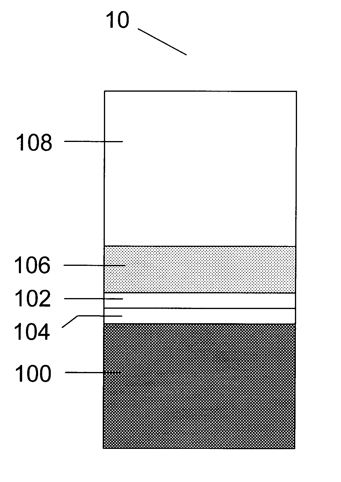
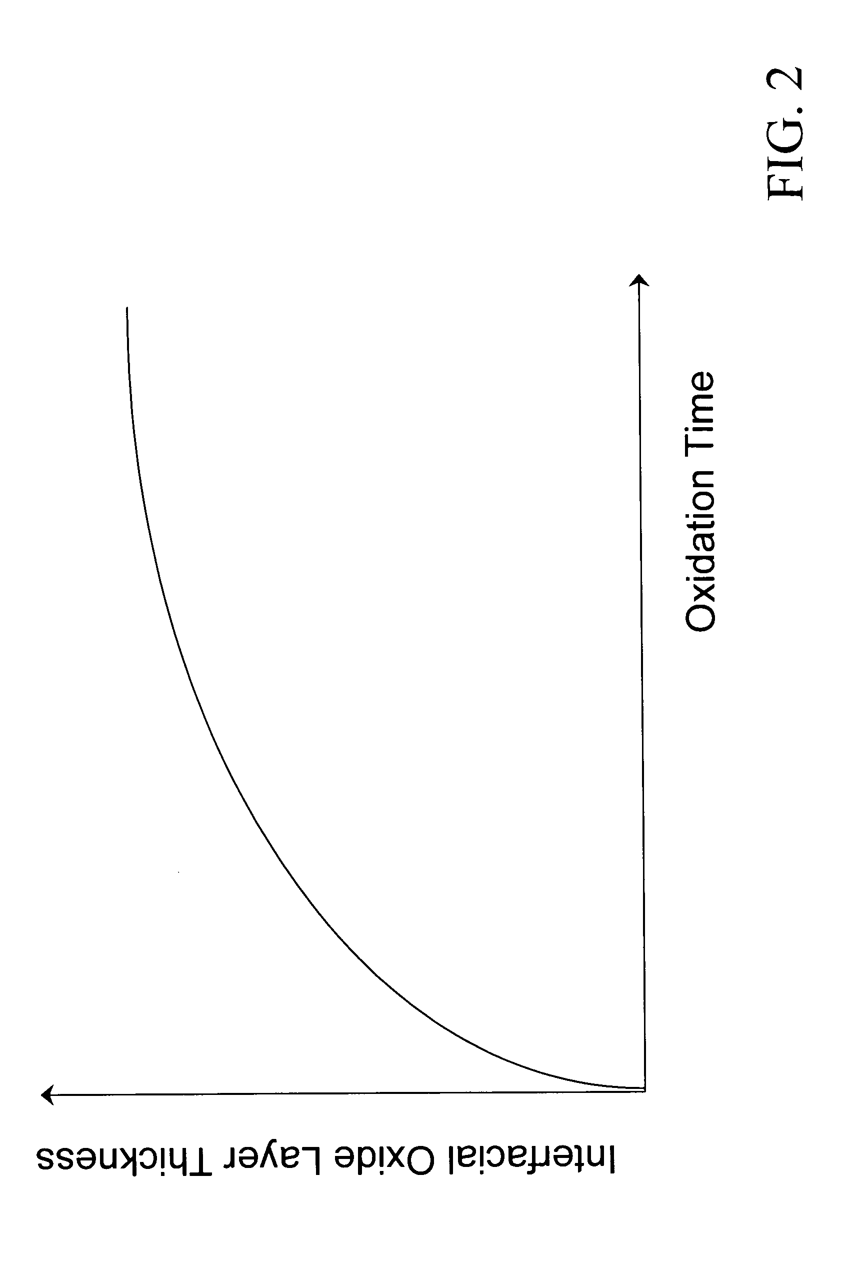
A method is provided for forming a microstructure with an interfacial oxide layer by using a diffusion filter layer to control the oxidation properties of a substrate associated with formation of a high-k layer into the microstructure. The diffusion filter layer controls the oxidation of the surface. The interfacial oxide layer can be formed during an oxidation process that is carried out following deposition of a high-k layer onto the diffusion filter layer, or during deposition of a high-k layer onto the diffusion filter layer.

Description

FIELD OF THE INVENTION[0001]The present invention relates to semiconductor processing, and more particularly, to a method of utilizing a diffusion filter layer to control substrate oxidation for integrating high-k dielectric layers into semiconductor manufacturing.BACKGROUND OF THE INVENTION[0002]In the semiconductor industry, the minimum feature sizes of microelectronic devices are approaching the deep sub-micron regime to meet the demand for faster, lower power microprocessors and digital circuits. The downscaling of CMOS devices imposes scaling constraints on the gate dielectric material. The thickness of the standard SiO2 gate dielectric oxide is approaching a level (˜10 angstrom (A)) at which tunneling currents may significantly impact transistor performance. To increase device reliability and reduce electron leakage from the gate electrode to the transistor channel, semiconductor transistor technology is using high-k gate dielectric materials that allow increased physical thic...

Claims


Application Information

Patent Timeline
Patent Type & Authority Patents(United States)
IPC IPC(8): H01L21/28H01L21/314H01L21/316H01L29/51
CPCH01L21/02181H01L21/02233H01L21/02238H01L21/02255H01L21/02271H01L21/02304H01L21/28185H01L21/3143H01L21/31658H01L21/31662H01L29/513H01L29/517H01L29/518H01L21/28194H01L21/28202H01L21/31604H01L21/31616H01L21/31637H01L21/31641H01L21/31645H01L21/022
Inventor O'MEARA, DAVID LWAJDA, CORYTAKAHASHI, TSUYOSHICALLEGARI, ALESSANDROSCHEER, KRISTENZAFAR, SUFIJAMISON, PAUL
Owner IBM CORP
Learn More