Dual band QWIP focal plane array

Inactive Publication Date: 2005-11-22
CALIFORNIA INST OF TECH
View PDF4 Cites 22 Cited by
  • Summary
  • Abstract
  • Description
  • Claims
  • Application Information

AI Technical Summary

Benefits of technology

[0018]The sensitivity of the detector is a function of efficiency of the photocurrent detection, i.e., the amount of detected photocurrent sensitivity is degraded by noise in the detector. Since infrared radiation has less energy than higher frequency electromagnetic radiation such as visible electromagnetic radiation, the system generates relatively less photocurrent. This has provided a unique challenge to enhancing detector efficiency.
[0058]The low voltage operation of the invention reduces power dissipation. Furthermore, the two-color QWIP FPA exhibits the same advantages as the single color QWIP FPAs discussed above. These include large size, uniform image, reproducible image, low cost, low 1 / f noise, and radiation hardness.

Problems solved by technology

This has provided a unique challenge to enhancing detector efficiency.
Dark current is a source of noise in QWIPs.
However, only some particles will tunnel through a barrier between 50 and 100 Å, and any barrier greater than 100 Å in thickness presents a formidable challenge for tunneling.
This produces its own special host of problems.
Without the absolute temperature, it is difficult to determine whether a given level of infrared input is emitted from a large and relatively cool object, or from a smaller, but hotter object.
One problem with separate FPA's is the need for two sets of optics, which significantly increases the size of the instrument.
Also, in high resolution applications, if the two FPA's are misregistered by even one pixel, the data becomes meaningless.
Hence, existing dual wavelength detectors have not generally performed satisfactorily, particularly in high resolution applications.
To the inventors' knowledge, this kind of QWIP structure has not yet been developed into a satisfactory focal plane array camera.
CMOS FPA readout multiplexers are needed to supply the voltages, but they cannot satisfactorily provide the required two voltage levels (e.g., 4V and 8V).
Another difficulty is that the LWIR segment of a two-stack QWIP FPA requires very high bias (greater than 8 volts) to switch on the LWIR detection.
Such high voltages are either not available in many applications, or when available, can overload circuits.
This is why QWIPs do not always respond well to normal incident light; it's also why large two dimensional FPAs usually require an optical coupling mechanism to couple the normal incident light into individual detectors.

Method used


Image

  • Dual band QWIP focal plane array
  • Dual band QWIP focal plane array
  • Dual band QWIP focal plane array

Examples


second embodiment

[0104]the invention is formed as described herein with reference to FIG. 6 to form the layered structure shown in FIG. 7. At step 600, a GaAs substrate of 630 μm is formed. This substrate is shown in FIG. 7 as substrate 700. The GaAs substrate 700 is preferable semi-insulating by virtue of being doped to N=5×1017 cm3. Stop etch layer 701 of 300 Å is also formed at step 601, covered by a 0.5 μm contact layer 701a formed at step 601a.

[0105]At step 602, molecular beam epitaxy (“MBE”) is used to form first a 500 Å barrier layer of AlxGa1-xAs layer 702 on the GaAs bottom contact layer 700. The layer 702 preferably has a thickness of 300–500 Å. This is followed by step 604 in which molecular beam epitaxy is used to form a 45 Å well 704 of GaAs. This process continues until 50 periods are formed. Each period so formed includes both a barrier and a well. One more barrier of undoped AlxGa1-xAs needs to be formed at step 605. Top contact layer 708 of GaAs is between 0.1–0.5 μm thick and appr...

first embodiment

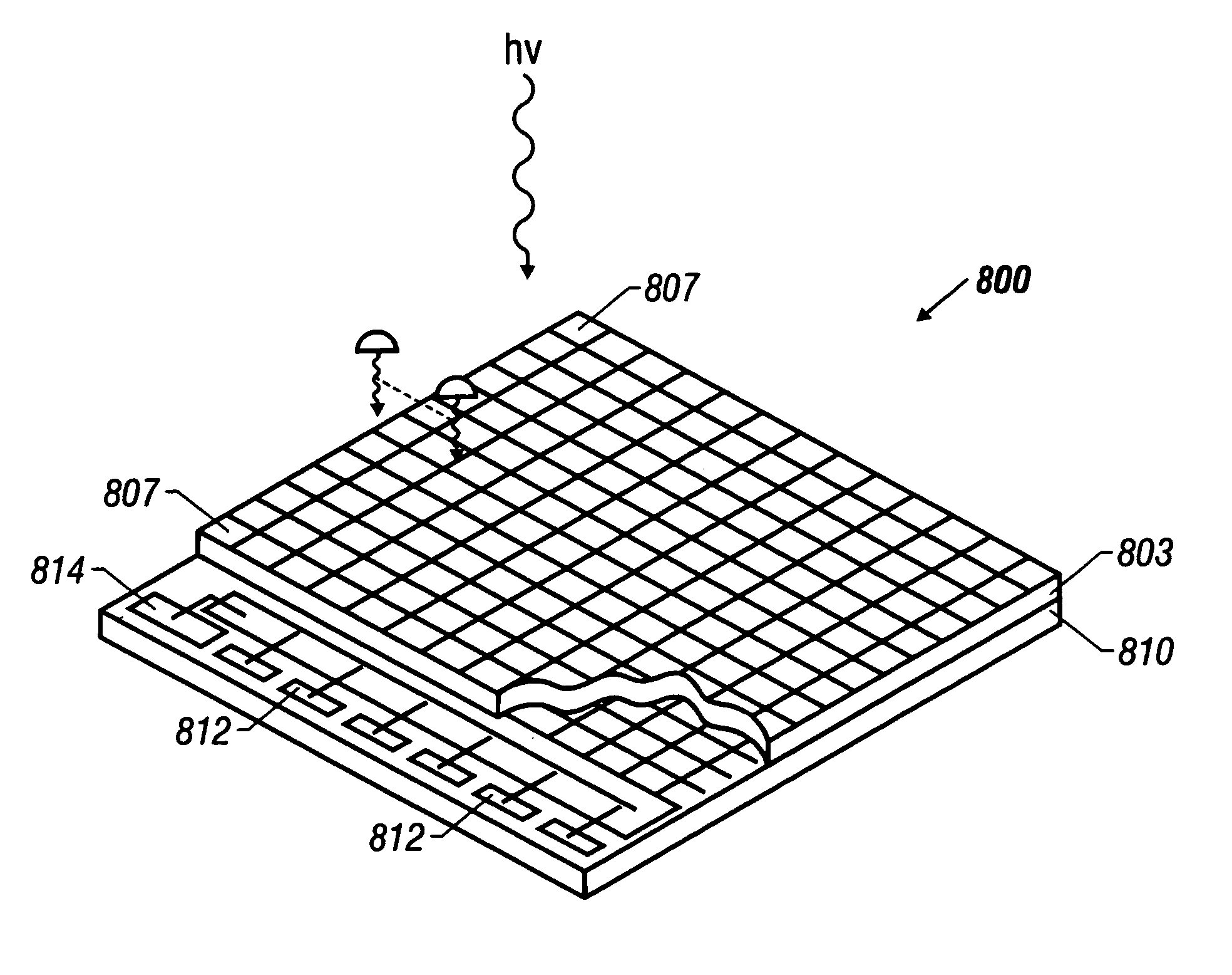
[0138]FIG. 14 shows a cross-sectional view of a QWIP 1350 of the invention. This embodiment includes substrate 1302, contact layer 1204 and GaAs layers 1208. Also, an LWIR stack 1202 and an MWIR stack 1200 are shown. A metal contact layer 1352 is disposed on top of the LWIR stack and a second metal contact 1354 is formed on top a portion of the MWIR stack 1200 which protrudes adjacent to the LWIR stack. A pair of indium bumps 1356 and 1358 are disposed on top of the respective metal contacts 1352 and 1354. Identical QWIP structures 1350 are arranged in columns and rows, one per pixel, as shown in FIG. 14.

[0139]In this embodiment, it is possible to read out both LWIR and MWIR outputs simultaneously by electrically addressing the indium bumps individually. This may be done using a hibridized multiplexer such as the multiplexer 810 shown in FIG. 8. Also, since each pixel is used for both colors, there is full spatial resolution.

[0140]FIGS. 15A–C show cross-sectional views of a single p...

third embodiment

[0148]FIG. 17A shows a schematic conduction band diagram of a two-color bound-to-quasibound QWIP 1700 of the present invention. This embodiment provides a smooth continuum transport band (with no steps) for photoexcited carriers from quantum wells responsive to both wavelengths. In this embodiment, the two wavelengths are two different LWIR wavelengths, such as 8.5 and 10.5 μm, referred to as LW1 and LW2 respectively.

[0149]A smooth continuum transport band is desirable in this embodiment because the two different wavelength QWIP structures are interlaced, in an alternating structure. With the LW1 and LW2 QWIPs next to each other, the smooth conductive band will prevent extra quantum mechanical reflections in the continuum transport band, which would otherwise occur if the transport band abruptly changed. The smooth transport band results from having a uniform barrier height between the different wavelength sensitive QWIPs in the two-color QWIP structure 1700. A uniform barrier heigh...


PUM


Abstract

A quantum well infrared photodetector (QWIP) that provides two-color image sensing. Two different quantum wells are configured to absorb two different wavelengths. The QWIPs are arrayed in a focal plane array (FPA). The two-color QWIPs are selected for readout by selective electrical contact with the two different QWIPs or by the use of two different wavelength sensitive gratings.

Description

CROSS-REFERENCE TO RELATED APPLICATION[0001]This application is a continuation of Ser. No. 08 / 928,292 Sep. 12, 1997 U.S. Pat. No. 6,642,537 which is a continuation-in-part of Ser. No. 08 / 708,076 Aug. 27, 1996 abandoned.ORIGIN OF THE INVENTION[0002]The invention described herein was made in the performance of work under a NASA Contract and is subject to the provisions of Public Law 95.517 (35 U.S.C. 202) in which the contractor has elected to retain title.FIELD OF THE INVENTION[0003]This invention relates to quantum-well devices for detecting infrared (“IR”) electromagnetic radiation.BACKGROUND AND SUMMARY[0004]Objects emit infrared radiation according to their temperature. An object at room temperature (i.e., 300° K), for example, emits infrared radiation that has a peak at around 8.5 μm. Even in complete darkness, i.e., in the absence of visible optical wavelengths, the infrared radiation emitted from the object can be detected. That detected radiation can be processed with an infr...

Claims


Application Information

Patent Timeline
IPC IPC(8): H01L27/146H01L31/08H01L31/09G01J5/28H01L31/0304H01L31/0352H01L31/103
CPCB82Y20/00G01J5/28H01L27/14652H01L31/035236H01L27/14634H01L27/14694H01L31/03046H01L31/1035Y10S977/759
Inventor GUNAPALA, SARATH D.CHOI, KWONG KITBANDARA, SUMITH V.
Owner CALIFORNIA INST OF TECH
Why Eureka
Try Eureka