Creating large bandwidth line defects by embedding dielectric waveguides into photonic crystal slabs

a dielectric waveguide and photonic crystal technology, applied in the field of waveguides in photonic crystals, can solve the problems of large group velocity dispersion, large guiding bandwidth of proposed waveguide structures, and none of the above-described approaches are entirely satisfactory, and achieve the effect of increasing the bandwidth of optical waveguides and large bandwidth

Inactive Publication Date: 2005-10-18
THE BOARD OF TRUSTEES OF THE LELAND STANFORD JUNIOR UNIV
View PDF4 Cites 2 Cited by
  • Summary
  • Abstract
  • Description
  • Claims
  • Application Information

AI Technical Summary

Benefits of technology

[0015]This invention is based on the observation that a large bandwidth optical waveguide can be achieved by placing in the slit of a photonic-crystal slab a dielectric waveguide has a dispersion that is substantially phase matched with a band gap of the slab to form the optical waveguide. Dimensions of the slab, the slit and / or the dielectric waveguide are preferably adjusted such that there is substantially a single mode in a band gap of the photonic-crystal slab. Preferably these dimensions are also chosen to increase the bandwidth of the optical waveguide.

Problems solved by technology

However, many of the proposed waveguide structures exhibit relatively small guiding bandwidth and large group velocity dispersion.
None of the above-described approaches are entirely satisfactory.

Method used


Image

  • Creating large bandwidth line defects by embedding dielectric waveguides into photonic crystal slabs
  • Creating large bandwidth line defects by embedding dielectric waveguides into photonic crystal slabs
  • Creating large bandwidth line defects by embedding dielectric waveguides into photonic crystal slabs

Examples


Embodiment Construction

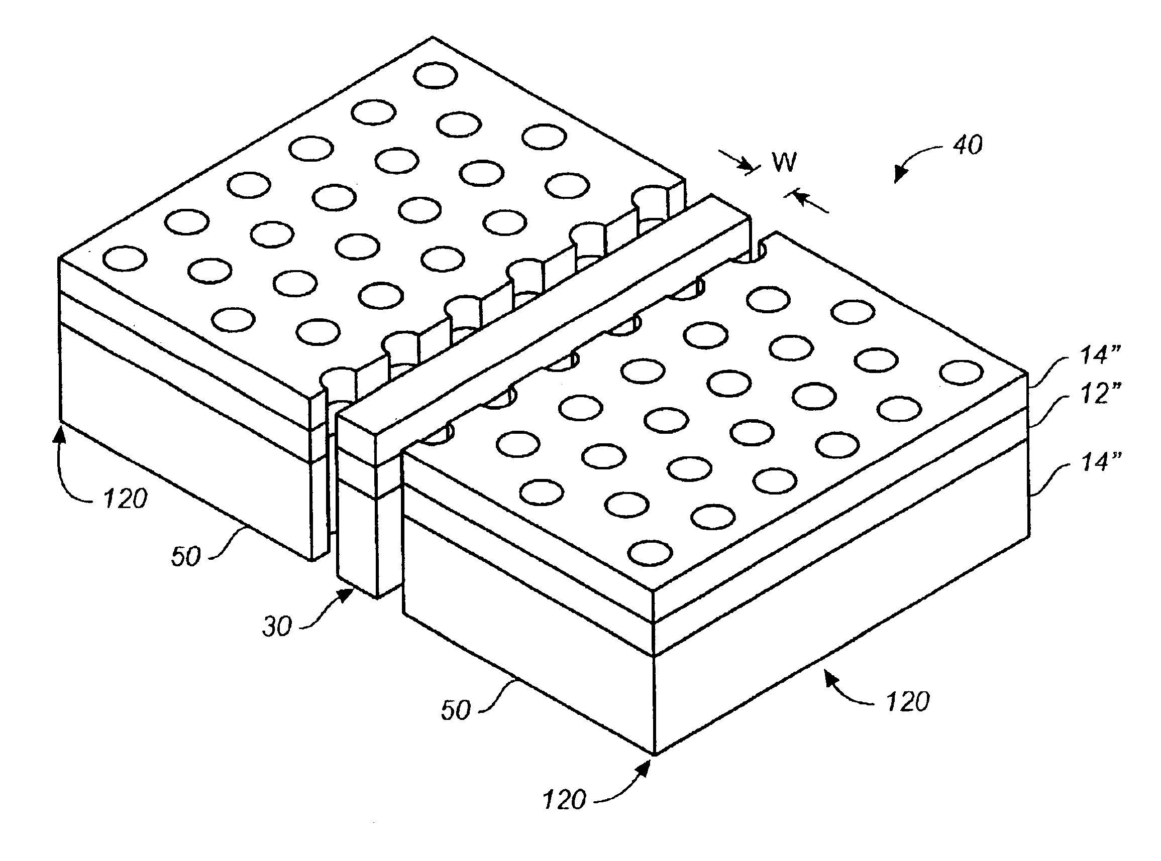
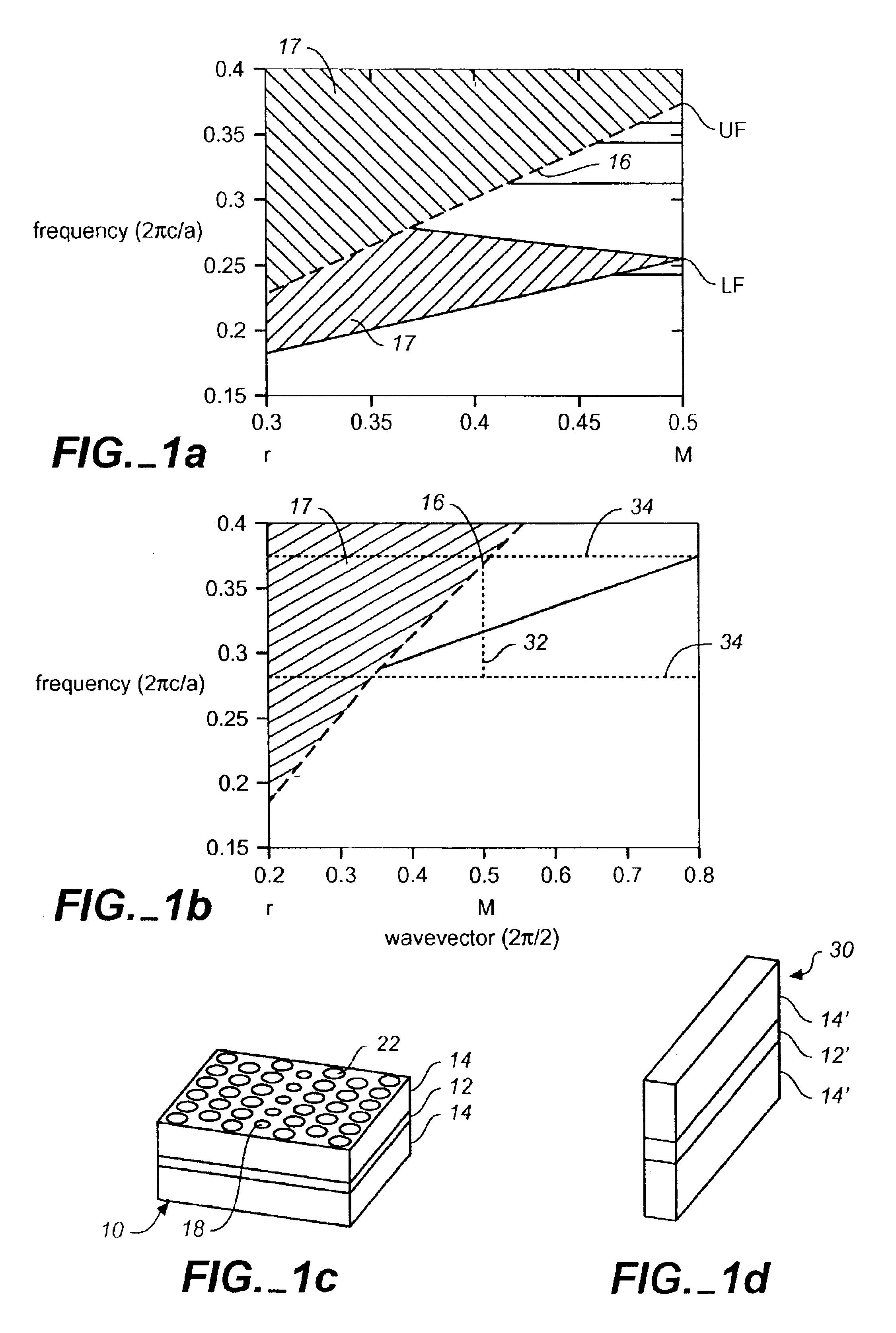
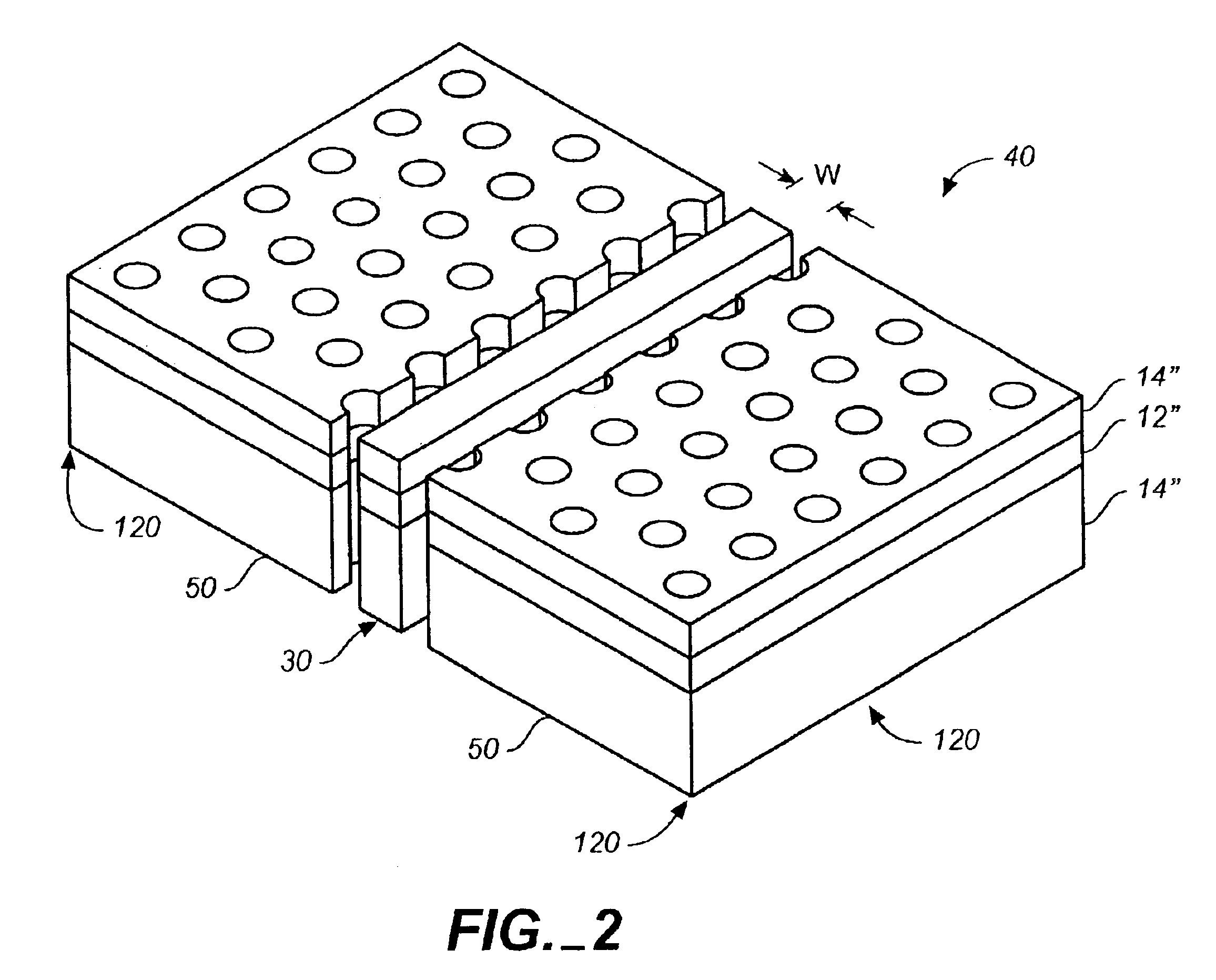
[0031]In this application, we introduce a general designing procedure that allows us, for any given photonic crystal slab, to create an appropriate waveguide structure that possesses single-mode bands with large bandwidth and low dispersion within the photonic band gap below the light line. In the preferred embodiment, the procedure comprises two steps: we first design a conventional dielectric waveguide that is optimally phase matched with the band gap of the photonic crystal slab. We then embed the dielectric waveguide into the photonic crystal in an appropriate way such that the edge states are eliminated and single mode propagation is preferably ensured. This procedure produces waveguide structures with large bandwidth of single mode and lossless propagation, and create dispersion relations that are essentially linear over most of the guiding bandwidth.

[0032]The underlying physical reasoning of our design is best illustrated by comparing the dispersion relation of a conventional...


PUM


Abstract

We introduce a general designing procedure that allows us, for any given photonic crystal slab, to create an appropriate line defect structure that possesses single-mode bands with large bandwidth and low dispersion within the photonic band gap region below the light line. This procedure involves designing a high index dielectric waveguide that is phase matched with the gap of the photonic crystal slab, and embedding the dielectric waveguide as a line defect into a crystal in a specific configuration that is free of edge states within the guiding bandwidth. As an example, we show a single mode line defect waveguide with a bandwidth approaching 13% of the center-band frequency, and with a linear dispersion relation throughout most of the bandwidth.

Description

CROSS REFERENCE TO RELATED APPLICATION[0001]This application claims the benefit of U.S. Provisional application Ser. No. 60 / 392,193, filed on Jun. 27, 2002.[0002]This work was supported in part by National Science Foundation under grant ECS-0200445. The government has rights in this application.BACKGROUND OF THE INVENTION[0003]This invention relates in general to waveguides in photonic-crystals and, in particular, to a structure where dielectric waveguides are incorporated in photonic crystal slabs.[0004]Photonic crystal slab structures are constructed by introducing strong two-dimensionally periodic refractive index contrast into a high-index dielectric guiding slab. See, for example, Two-dimensional photonic-bandgap structures operating at near-infrared wavelengths, by T. F. Kraus, R. M. DelaRue, and S. Brand, Nature 383, 699 (1996). With sufficient refractive index contrast in the vertical direction, such structures support an in-plane photonic band gap that lies below the light ...

Claims


Application Information

Patent Timeline
Patent Type & Authority Patents(United States)
IPC IPC(8): G02B6/122
CPCB82Y20/00G02B6/1225
Inventor LAU, WAH TUNGFAN, SHANHUI
Owner THE BOARD OF TRUSTEES OF THE LELAND STANFORD JUNIOR UNIV
Why Eureka
Try Eureka