Plasma processing apparatus

Inactive Publication Date: 2005-10-11
TOKYO ELECTRON LTD +1
View PDF20 Cites 11 Cited by
  • Summary
  • Abstract
  • Description
  • Claims
  • Application Information

AI Technical Summary

Benefits of technology

[0015]Another object of the present invention is to provide a plasma processing apparatus which not only can suppress the production of dust, particles, etc., but also can suppress the surface wave plasma which is harmful to the plasma processing procedure.
[0016]As a result of earnest study, the present inventors have found that the provision of a specific shape to a dielectric material to be disposed between antenna means for guiding microwave, and a plasma processing chamber is extremely effective for attaining the above-mentioned object.

Problems solved by technology

When such surface wave is generated, surface wave plasma (SWP) is also generated in the inside of the plasma processing chamber, and there occurs a problem that a mode peculiar to the wave motion is provided.
However, when a metal member is disposed in the plasma boundary region, unnecessary dust, particles, etc., are produced in the plasma processing chamber due to the sputtering phenomenon in the site where the plasma comes into contact with the metal member, whereby the process performance of the plasma processing can be greatly deteriorated.

Method used


Image

  • Plasma processing apparatus
  • Plasma processing apparatus
  • Plasma processing apparatus

Examples


Embodiment Construction

[0030]Hereinbelow, the present invention will be described in detail with reference to the accompanying drawings, as desired. In the following description, “%” and “part(s)” representing a quantitative proportion or ratio are those based on mass, unless otherwise noted specifically.

[0031](Plasma Processing Apparatus)

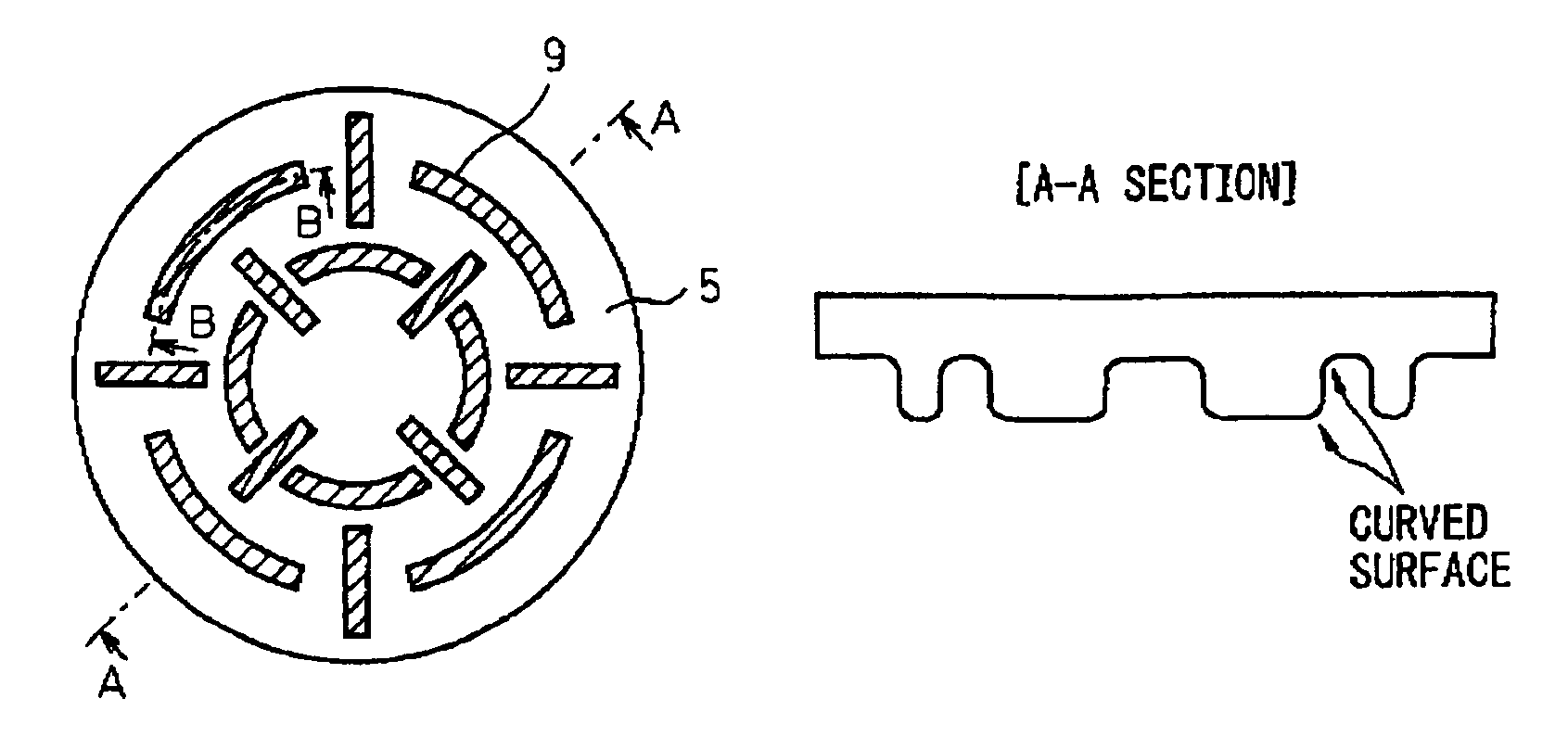
[0032]The plasma processing apparatus according to the present invention basically comprises: at least, a plasma processing chamber for processing therein an object to be processed; antenna means for guiding microwave into the plasma processing chamber; and a dielectric member disposed between the antenna means and the plasma processing chamber. This plasma processing apparatus is characterized in that a projecting shape is provided in the above-mentioned dielectric member facing the inside of the plasma processing chamber.

[0033](One Embodiment of Plasma Processing Apparatus)

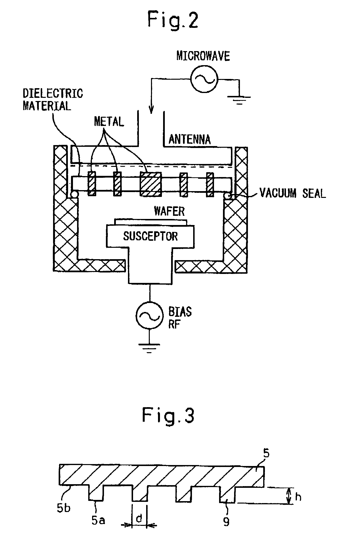
[0034]FIG. 1 is a schematic sectional view showing a preferred embodiment of the plasma processin...


PUM


Abstract

A plasma processing apparatus, comprising: at least, a plasma processing chamber for processing therein an object to be processed; antenna means for guiding microwaves into the plasma processing chamber; and a dielectric member disposed between the antenna means and the plasma processing chamber; wherein a surface of the dielectric member facing the inside of the plasma processing chamber has a projecting shape.

Description

BACKGROUND OF THE INVENTION[0001]1. Field of the Invention[0002]The present invention relates to a plasma processing apparatus which is suitably usable when an object to be processed is subjected to various plasma treatments for the purpose of manufacturing an electronic device, etc.[0003]2. Background Art[0004]In general, a plasma processing apparatus according to the present invention is widely applicable to various kinds of plasma processing procedures, which include the production of materials for electronic device such as semiconductors or semiconductor devices, and liquid crystal devices. For the convenience of explanation, however, the background art relating to semiconductor devices will be described below.[0005]In general, in the processes for manufacturing semiconductor devices, a base material or substrate (such as wafer) for semiconductor devices as an object to be processed is subjected to various kinds of treatments such as CVD (chemical vapor deposition), etching, and...

Claims


Application Information

Patent Timeline
IPC IPC(8): H01J37/32H01L21/00H05B6/80B01J19/08H05H1/46C23C16/44C23C16/511H01L21/205H01L21/3065
CPCH01J37/32192H01L21/67069H05B6/72H05B6/806
Inventor ISHII, NOBUOYASAKA, YASUYOSHI
Owner TOKYO ELECTRON LTD
Why Eureka
Try Eureka