Method for manufacturing a single electron memory device having quantum dots between gate electrode and single electron storage element

Inactive Publication Date: 2005-09-20
SAMSUNG ELECTRONICS CO LTD
View PDF10 Cites 19 Cited by
  • Summary
  • Abstract
  • Description
  • Claims
  • Application Information

AI Technical Summary

Benefits of technology

[0018]A feature of an embodiment of the present invention provides a single electron memory device having quantum dots or an element having the same effect, which retains information long enough to be practical and prevents variation in the properties of the device.
[0033]The single electron memory device according to an embodiment of the present invention includes a silicon nitride layer as a nano-scale storage medium between quantum dots, which are included on the bottom surface of a gate electrode, and a tunneling layer formed on a nano-scale channel region. As a result, the silicon nitride layer may be locally charged even in a nano-scale, and may retain information longer than a conventional single electron memory device using quantum dots as a data storage electrode. Further, in the present invention, the quantum dots are not included on a lower layer as a tunneling layer, but in an upper layer, thereby maintaining the properties of a device and allowing the quantum dots to be formed by various methods.

Problems solved by technology

As the size of a metal-oxide-semiconductor field effect transistor (MOSFET) becomes smaller, problems arise that do not occur in larger devices.
Thus, it becomes difficult to further reduce the size of the MOSFET.
For example, as the size of the MOSFET device becomes smaller, problems occur such as lowering of threshold voltage caused by a decrease in effective channel length, drain induced barrier lowering (DIBL), punch-through, deterioration of a gate oxide layer, and an increase in leakage current due to hot carriers generated by an increase in the electrical field in the device.
These problems complicate further reduction in the size of a MOSFET.
The most significant problem to be solved by continuously scaling the MOSFET to the range of nanometers (nm) is a physical limit.
Thus, proper operation of a miniaturized MOSFET at room temperature is not expected.
In the conventional single electron memory devices, however, the quantum dot or the nano-crystal array is formed directly on the tunneling oxide layer 12, and thus, defects may occur in the tunneling oxide layer 12 while forming the quantum dot or the nano-crystal array.
These defects may result in changes in the properties of the device thereby requiring many limitations in the formation of the quantum dot on the tunneling oxide layer 12.
It is difficult, however, to form the quantum dot having a predetermined size due to the possibility of causing defects in the tunneling oxide layer.
Hence, it becomes difficult to manufacture a single electron memory device, which operates at room temperature.
Further, in the prior art single electron memory device, the retention time of information does not reach a practical standard.

Method used


Image

  • Method for manufacturing a single electron memory device having quantum dots between gate electrode and single electron storage element
  • Method for manufacturing a single electron memory device having quantum dots between gate electrode and single electron storage element
  • Method for manufacturing a single electron memory device having quantum dots between gate electrode and single electron storage element

Examples


first embodiment

[0045

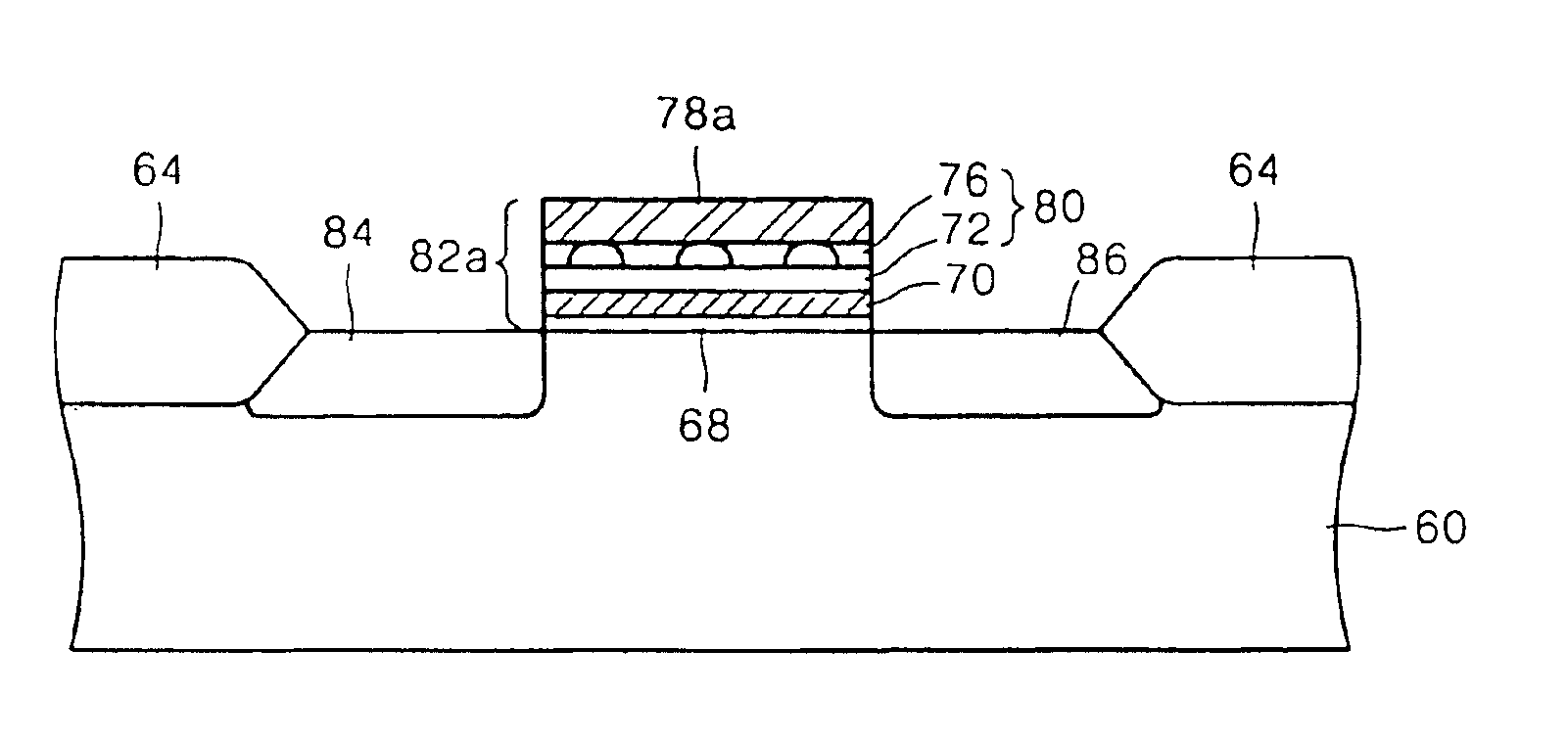
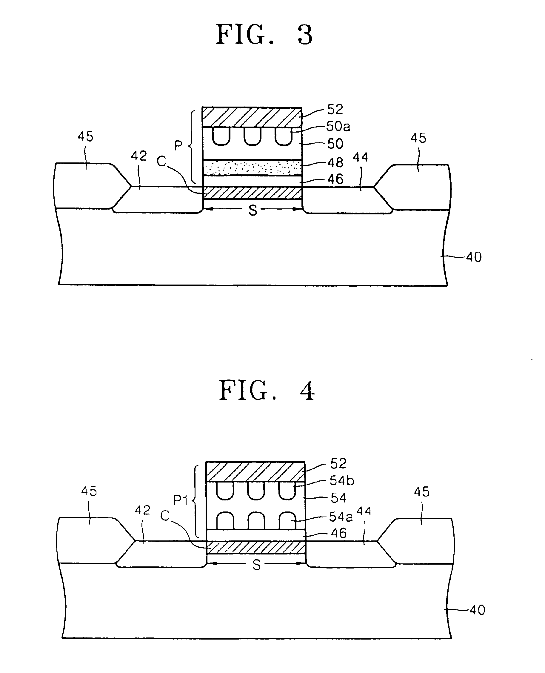
[0046]Referring to FIG. 3, reference numeral 40 denotes a substrate on which a MOSFET is formed. The substrate 40 may be a P-type or N-type semiconductor substrate, for example, a silicon substrate, depending on the type of the MOSFET. Reference numerals 42 and 44 denote first and second conductive impurity regions, which are formed on the substrate 40. More particularly, the first and second conductive impurity regions are a source region and a drain region. Reference numeral 45 denotes a field oxide layer, more particularly, a LOCOS-type oxide layer. The first and second conductive impurity regions 42 and 44 are spaced apart from each other by a distance S, preferably several tens of nanometers (nm). As a result, the scale of a channel region C formed on the upper portion of the substrate 40 between the first and second conductive impurity regions 42 and 44 is in nano-scale.

[0047]A gate lamination pattern P is formed on the channel region C. The gate lamination pattern P incl...

second embodiment

[0058

[0059]The single electron memory device according to a second embodiment of the present invention is a single electron storage means using quantum dots.

[0060]In detail, referring to FIG. 4, a gate lamination pattern P1 is formed on the channel region C of a substrate 40. The gate lamination pattern P1 includes a lower layer 46, an upper layer 54, and a gate electrode 52, which are sequentially formed on the channel region of a substrate 40. A plurality of vertically spaced-apart first and second quantum dots 54a and 54b are included in the upper layer 54. The first quantum dots 54a are formed on the lower layer 46 at a predetermined interval. The second quantum dots 54b are formed above the first quantum dots 54a and are in contact with the bottom surface of the gate electrode 52. The first quantum dots 54a function as the single electron storage medium (48 of FIG. 3) of the first embodiment.

third embodiment

[0061

[0062]As shown in FIG. 5, the structure of the single electron memory device according to the third embodiment is similar to the structure of the single electron memory device according to the first embodiment. However, in the third embodiment, the quantum dots 50a, included between a gate electrode 52 and a single electron storage medium 48, are not only in contact with the bottom surface of the gate electrode 52 but are also in contact with the single electron storage medium 48. In this case, since the gate electrode 52 locally contacts the nano-scale single electron storage medium 48, the local charging rate of the single electron storage medium 48 may increase.


PUM


Abstract

In a method for manufacturing a single electron memory device including a single electron storage element in a gate lamination pattern formed on a nano-scale channel region of a MOSFET, formation of the gate lamination pattern includes sequentially forming a lower layer and a single electron storage medium for storing a single electron tunneling through the lower layer on a substrate, forming an upper layer including a plurality of quantum dots on the single electron storage medium, forming a gate electrode layer on the upper layer to be in contact with the plurality of quantum dots, and patterning the lower layer, the single electron storage medium, the upper layer, and the gate electrode layer, in reverse order.

Description

[0001]This application is a DIVISION of application Ser. No 10 / 125,597, filed Apr. 19, 2002 now U.S. Pat. No. 6,670,670.BACKGROUND OF THE INVENTION[0002]1. Field of the Invention[0003]The present invention relates to a memory device and method for manufacturing the same. More particularly, the present invention relates to a single electron memory device having quantum dots between a gate electrode and a single electron storage element and method for manufacturing the same.[0004]2. Description of the Related Art[0005]As the size of a metal-oxide-semiconductor field effect transistor (MOSFET) becomes smaller, problems arise that do not occur in larger devices. Thus, it becomes difficult to further reduce the size of the MOSFET. For example, as the size of the MOSFET device becomes smaller, problems occur such as lowering of threshold voltage caused by a decrease in effective channel length, drain induced barrier lowering (DIBL), punch-through, deterioration of a gate oxide layer, and ...

Claims


Application Information

Patent Timeline
IPC IPC(8): H01L21/28H01L29/66H01L21/02H01L29/788G11C16/04H01L21/8247H01L27/10H01L29/792
CPCB82Y10/00H01L21/28273H01L29/7888G11C2216/08H01L29/40114H01L29/788
Inventor CHAE, SOO-DOOKIM, BYONG-MANKIM, MOON-KYUNGCHAE, HEE-SOONRYU, WON-IL
Owner SAMSUNG ELECTRONICS CO LTD
Why Eureka
Try Eureka