
Method for real time metal ETCH critical dimension control

a metal etching and critical dimension technology, applied in the direction of mechanical measuring arrangements, semiconductor/solid-state device testing/measurement, instruments, etc., can solve the problems of etch tool performance changing with time, each wafer lot etches somewhat differently, and the fabrication of semiconductor integrated circuits requires an increasingly expensive and tightly controlled process s

Inactive Publication Date: 2005-09-06
NAT SEMICON CORP
View PDF8 Cites 6 Cited by
  • Summary
  • Abstract
  • Description
  • Claims
  • Application Information

AI Technical Summary

Benefits of technology

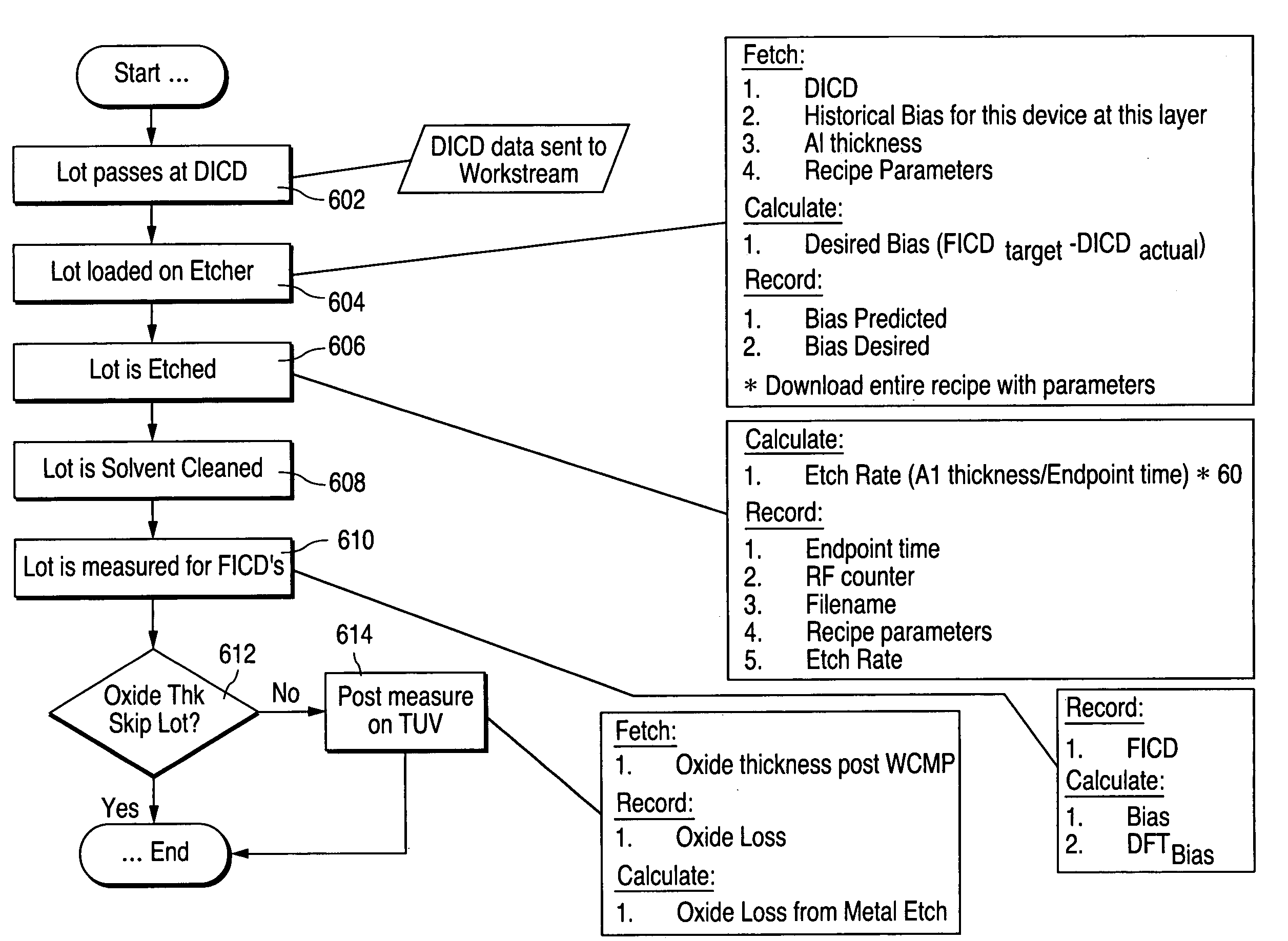
[0014]The present invention provides the ability to target FICD's to account for inherent variability in incoming conditions and chamber level specifics due to the age of the etch chamber and other subtle differences. The invention provides both real time control of the etch process through an automated system that does not rely on human intervention and the ability to track etch tool performance based upon expected / predicted results.

Problems solved by technology

The fabrication of semiconductor integrated circuits requires an increasingly expensive and integrated set of tightly controlled processes to obtain the desired critical dimensions (CD) of the physical integrated circuit features within acceptable product yield.
This conventional method of control suffers from the disadvantages that every wafer lot etches somewhat differently and etch tool performance changes with time.

Method used


Image

  • Method for real time metal ETCH critical dimension control
  • Method for real time metal ETCH critical dimension control
  • Method for real time metal ETCH critical dimension control

Examples


Embodiment Construction

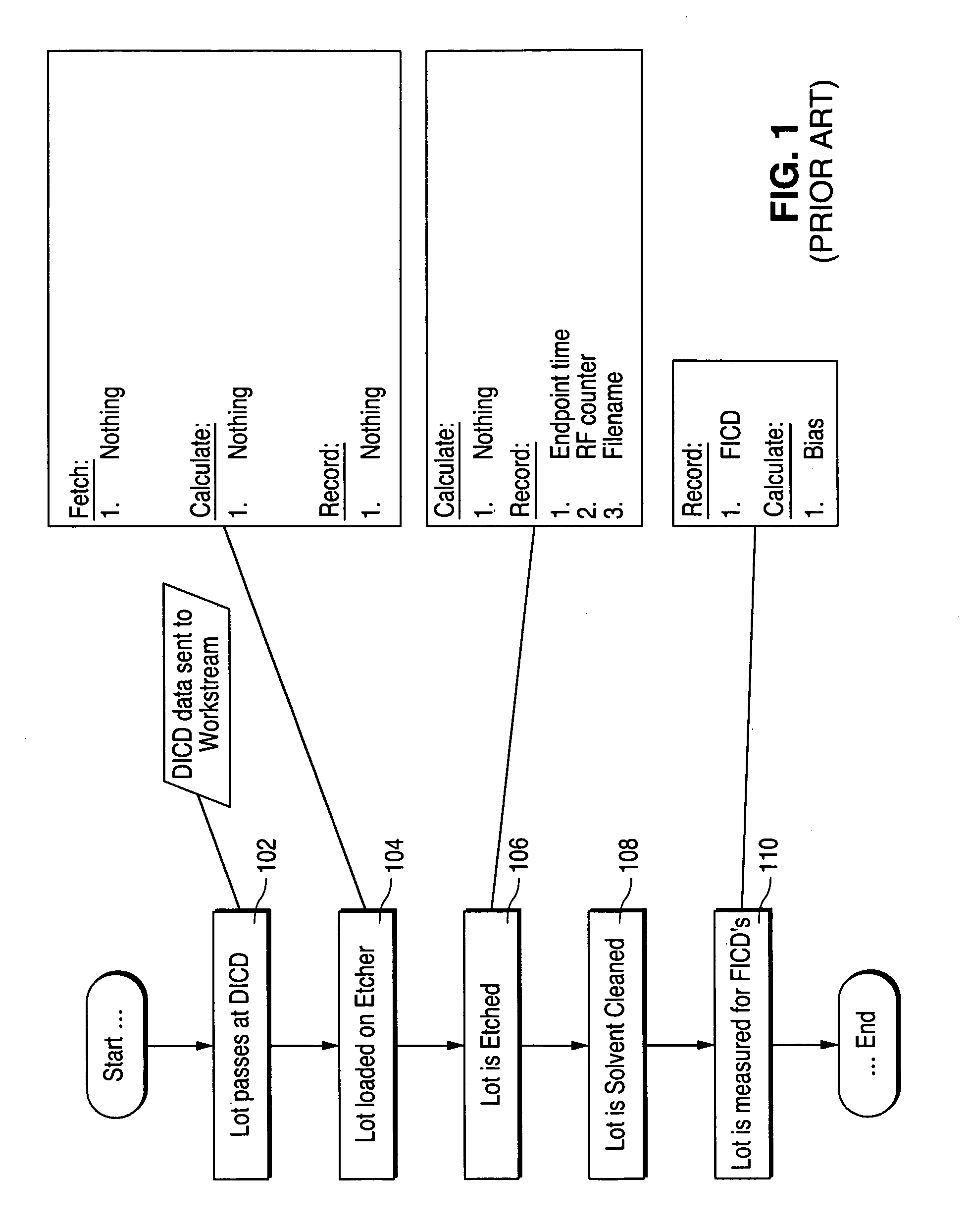
[0022]As discussed above, currently, metal line etch relies totally on DICD targeting to hit FIDC targets. In accordance with the present invention, bias targeting is used to provide an opportunity at the metal etch step to compensate for variability in incoming conditions such as DICD and to use the historical bias on a reticle / tool combination and the current etch tool performance to improve process control and, ultimately, Cpk and final wafer yields. That is, a method in accordance with the present invention uses subtle recipe changes to gases and / or power to move a reticle bias away from historical values to better target FIDC.

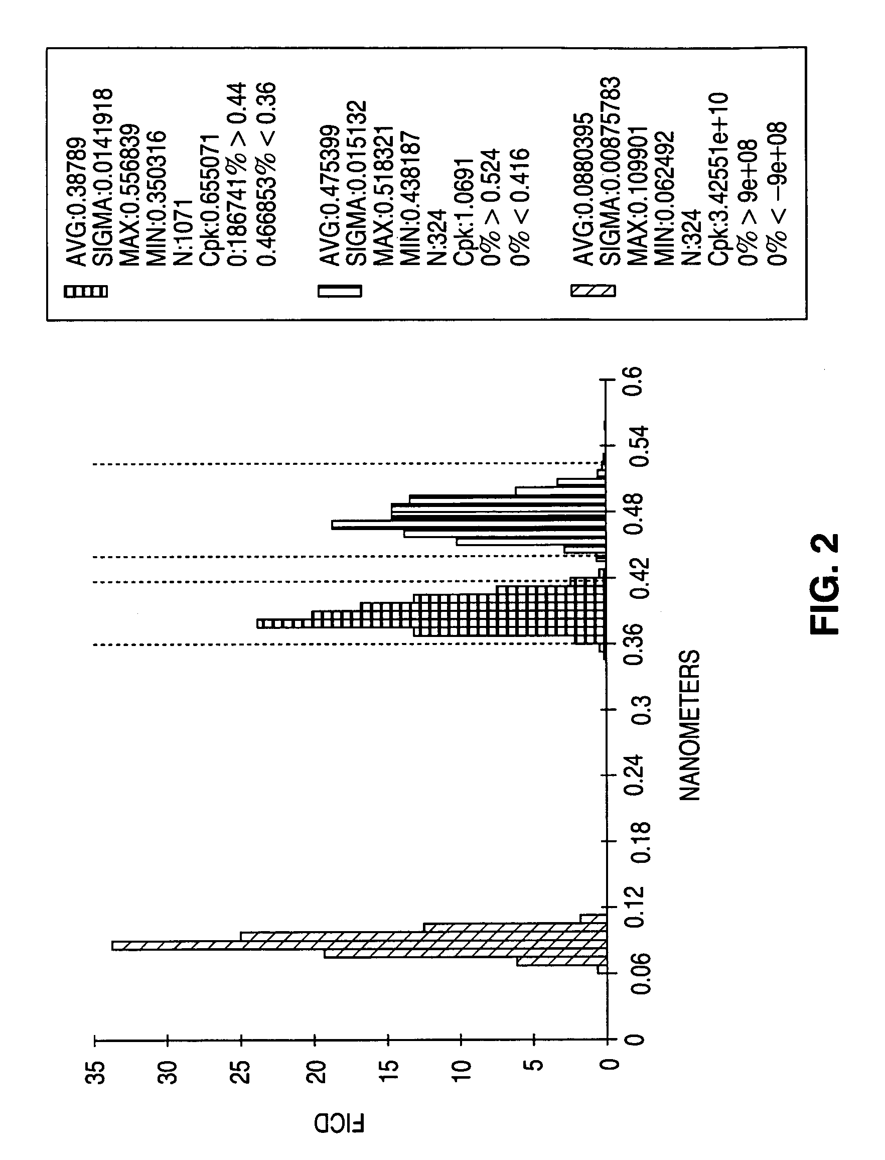
[0023]As can be seen from the FIG. 2 histogram, bias generally has a tighter distribution than DI and FI for a technology layer / combination (metal 3 in a CMOS process, in the case of FIG. 2). In this case, sigma is roughly 40% less than DI or FI. Using this predictability to account for variations in DICD, FICD can be tightened.

[0024]The FIG. 3 plot provid...


PUM

PropertyMeasurementUnit
thicknessaaaaaaaaaa
etch rateaaaaaaaaaa
Critical Dimensionaaaaaaaaaa

Abstract

The present invention predicts Critical Dimension (CD) before processing a wafer lot and alters the etch by adjusting recipe inputs to control the current lots bias to target critical dimensions. Also, the process incorporates the use of etch chamber selection by an automated system, disallowing processing of a lot if critical dimensions are predicted to be out of control. Line caper, the angle of sidewall on the metal line, and oxide loss, the amount of oxide removed by the over etch portion of the process, are also used to monitor current tool performance and make adjustments to recipe inputs.

Description

TECHNICAL FIELD OF THE INVENTION[0001]The present invention relates to integrated circuit fabrication techniques and, in particular, to an integrated circuit fabrication method that incorporates critical dimension control using recent historical outputs together with current etch chamber performance data.DEFINITIONS[0002]As used herein, the following terms shall have the stated meaning:[0003]CD: Critical Dimension.[0004]Develop Inspect Critical Dimension (DICD): The line width of a photoresist mask pattern prior to etching.[0005]Final Inspect Critical Dimension (FICD): The line width of the final etched line in an integrated circuit structure.[0006]Bias: The difference between the Develop Inspect Critical Dimension (DICD) and the Final Inspect Critical Dimension (FICD).[0007]Reticle: A mask used to impart an image onto a wafer surface; the mask contains the integrated circuit device design specifics.[0008]Lot: A tracking number given to a quantity of integrated circuit wafers that t...

Claims


Application Information

Patent Timeline
Patent Type & Authority Patents(United States)
IPC IPC(8): G01B1/00H01L21/66
CPCH01L22/20
Inventor GRIFFIN, JUSTIN
Owner NAT SEMICON CORP
Learn More