Manufacturing method for a liquid crystal display device
a liquid crystal display and manufacturing method technology, applied in the direction of identification means, instruments, optics, etc., can solve the problems of film climb-over damage, increase in the number of manufacturing processes, and decrease in yield factor, so as to reduce the entire manufacturing process and reduce the effect of the entire manufacturing process
- Summary
- Abstract
- Description
- Claims
- Application Information
AI Technical Summary
Benefits of technology
Problems solved by technology
Method used
Image
Examples
embodiment 1
>
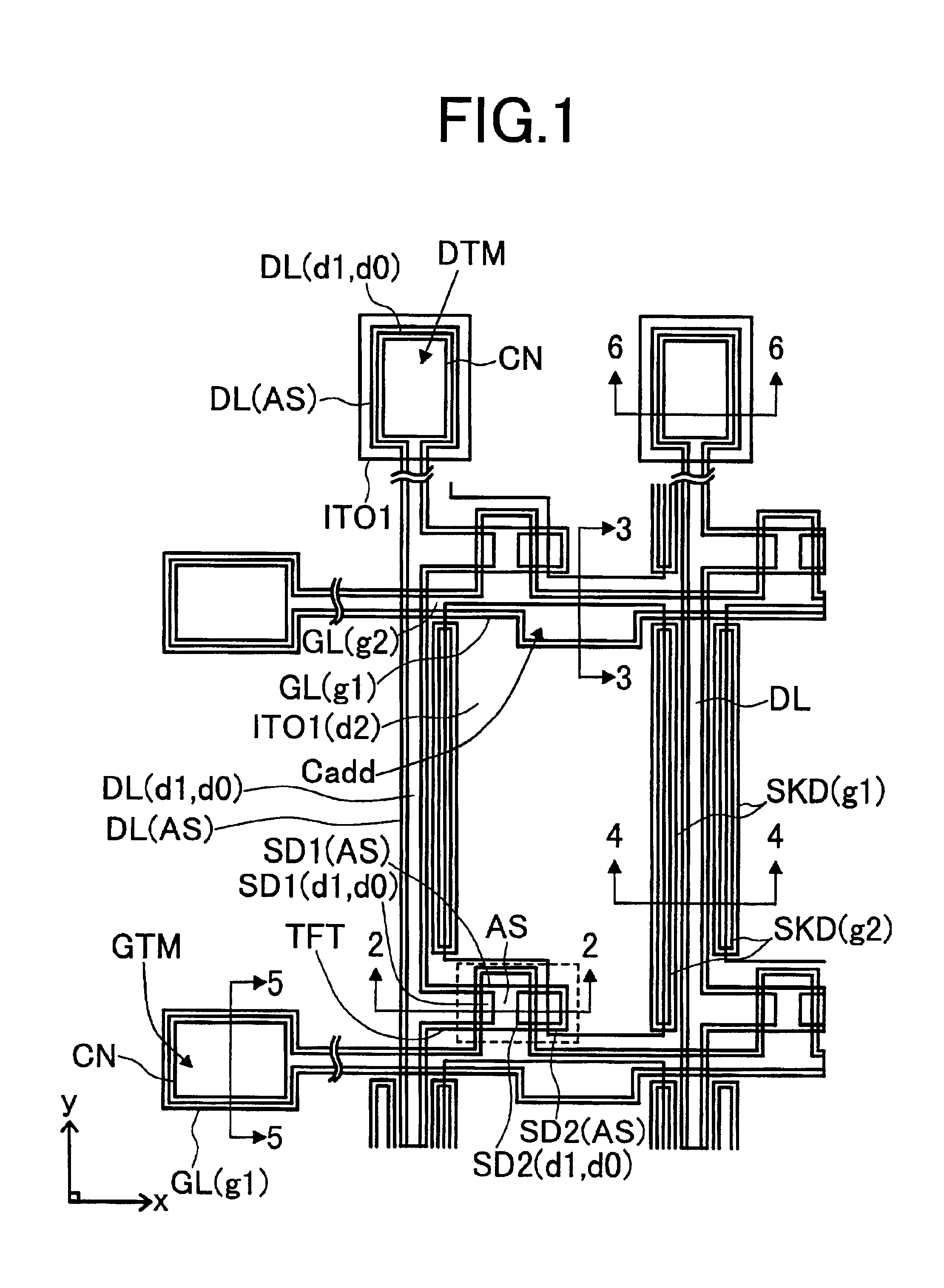
[0078]FIG. 54 is an equivalent circuit diagram showing one embodiment of the liquid crystal display device according to the invention. FIG. 54 is a circuit diagram which is depicted to correspond to the actual geometrical layout of the liquid crystal display device.
[0079]In FIG. 54, there is shown a transparent substrate SUB1. This transparent substrate SUB1 is disposed to be opposed to another transparent substrate SUB2 with a liquid crystal interposed therebetween.
[0080]Gate signal lines GL and drain signal lines DL are formed on a liquid-crystal-side surface of the transparent substrate SUB1. The gate signal lines GL are disposed to be extended in the x direction and to be juxtaposed in the y direction as viewed in FIG. 54, while the drain signal lines DL are insulated from the gate signal lines GL and are disposed to be extended in the y direction and to be juxtaposed in the x direction as viewed in FIG. 54. Rectangular areas each of which is surrounded by adjacent ones of the ...
embodiment 2
[0172]In the above description of Embodiment 1, reference has been made to the liquid crystal display device in which the thin film transistors TFT are formed by using the resist reflow method. However, the invention can also be applied to a liquid crystal display device in which its thin film transistors TFT are formed by using a so-called half-exposure method.
[0173]Embodiment 2 is the same as Embodiment 1 except the following construction.
>
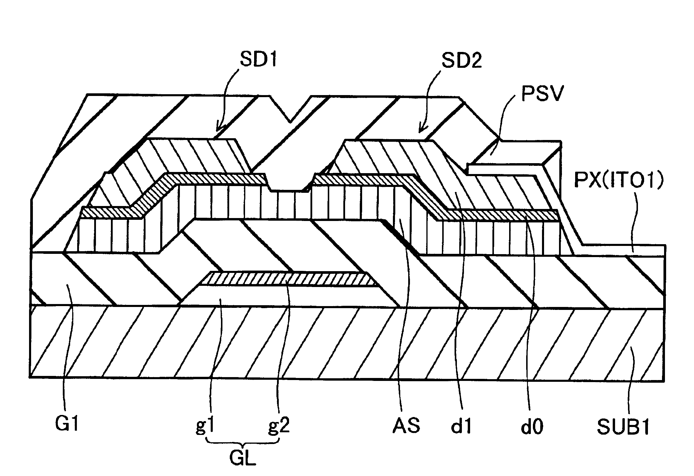
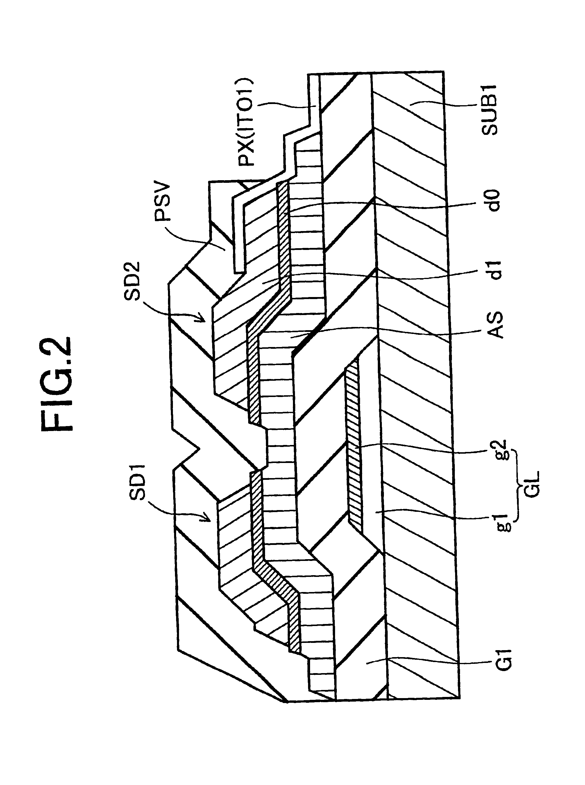
[0174]FIG. 11 is a view showing a cross section of a thin film transistor TFT formed by using a so-called half-exposure method.
[0175]The thin film transistor TFT has side walls formed by a stacked structure in which a semiconductor layer AS, a high-concentration layer d0 and a Mo layer d1 are stacked in that order, and the respective side walls are formed to have gently tapered surfaces which become gradually more open toward the transparent substrate SUB1.
[0176]FIGS. 15A to 15E are process diagrams showing one embodiment of a method of forming ...
embodiment 3
[0195]The invention can also be applied to a liquid crystal display device in which its thin film transistors TFT are formed by using a so-called ITO mask method.
[0196]Embodiment 3 is the same as Embodiment 1 except the following construction.
>
[0197]FIG. 18 is a view showing a cross section of a thin film transistor TFT formed by using an ITO mask method.
[0198]In the thin film transistor TFT, the ITO film ITO1 of the pixel electrode PX is directly superposed on not only the entire surface of the source electrode SD2, but also the surface of the drain signal line DL (and the drain electrode SD1).
[0199]Similarly to the case of the other embodiments, the side walls of a stacked structure in which the semiconductor layer AS, the high-concentration layer d0 and the Mo layer d1 are stacked in that order are respectively formed to have gently tapered surfaces which become gradually more open toward the transparent substrate SUB1.
[0200]FIGS. 22A to 22G are process diagrams showing one embod...
PUM
| Property | Measurement | Unit |
|---|---|---|
| transparent conductive | aaaaa | aaaaa |
| concentration | aaaaa | aaaaa |
| time | aaaaa | aaaaa |
Abstract
Description
Claims
Application Information
 - R&D
- Intellectual Property
- Life Sciences
- Materials
- Tech Scout
- Unparalleled Data Quality
- Higher Quality Content
- 60% Fewer Hallucinations
Browse by: Latest US Patents, China's latest patents, Technical Efficacy Thesaurus, Application Domain, Technology Topic, Popular Technical Reports.
© 2025 PatSnap. All rights reserved.Legal|Privacy policy|Modern Slavery Act Transparency Statement|Sitemap|About US| Contact US: help@patsnap.com


