Method for the production of an electronic component

a technology of electronic components and manufacturing methods, applied in the direction of printed element electric connection formation, conductive pattern formation, non-metallic protective coating applications, etc., can solve the problems of affecting the reliability of the closure of the via, and achieve the effect of avoiding contamination of the bottom side of the support body and low cos

Inactive Publication Date: 2005-08-16
CONTI TEMIC MICROELECTRONIC GMBH
View PDF30 Cites 14 Cited by
  • Summary
  • Abstract
  • Description
  • Claims
  • Application Information

AI Technical Summary

Benefits of technology

[0015]Following the application of the further metallizing layer forming the final metallization, the components of the circuit arrangement are soldered to the top side of the support body, for example by means of a reflow soldering process. Due to the closure of the vias and due to the secure anchoring of the screening material provided in the vias for the closure of the vias, contaminations of the bottom side of the support body can be avoided, particularly contaminations caused by a through flow of solder from the top side to the bottom side of the support body through the vias. The heat transport from the top side to the bottom side of the support body is not impaired by the screen printing material closing the vias and by the passivating layer applied to the bottom side of the support body.
[0016]In connection with the present safe and simple method for producing an electronic package, it is possible to advantageously prevent, at low costs, for all electrical and ther

Problems solved by technology

Such bubbles or fractures would impair th

Method used


Image

  • Method for the production of an electronic component
  • Method for the production of an electronic component
  • Method for the production of an electronic component

Examples


Embodiment Construction

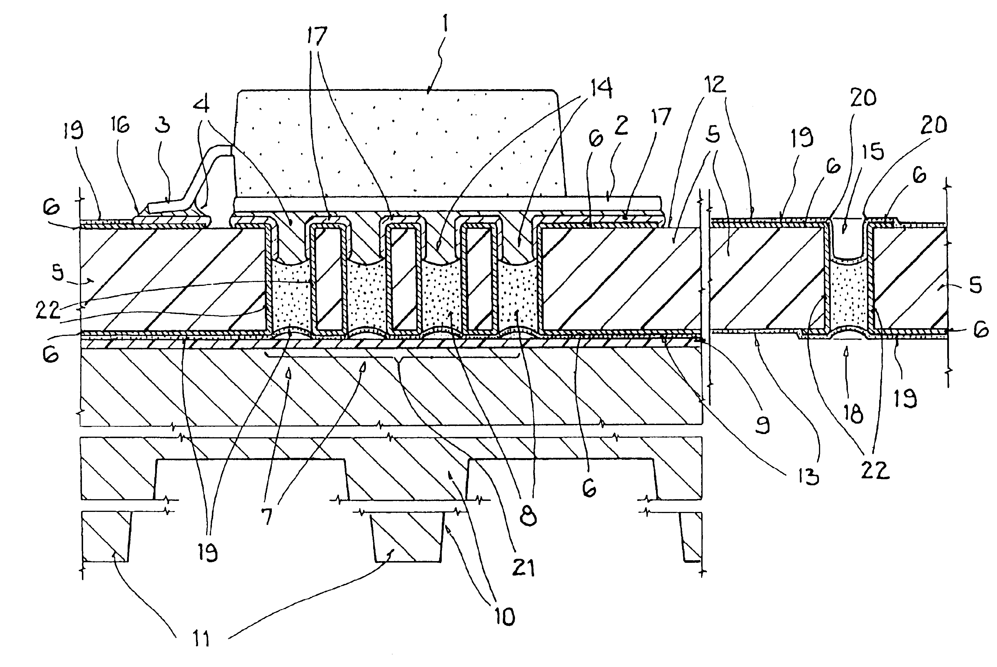
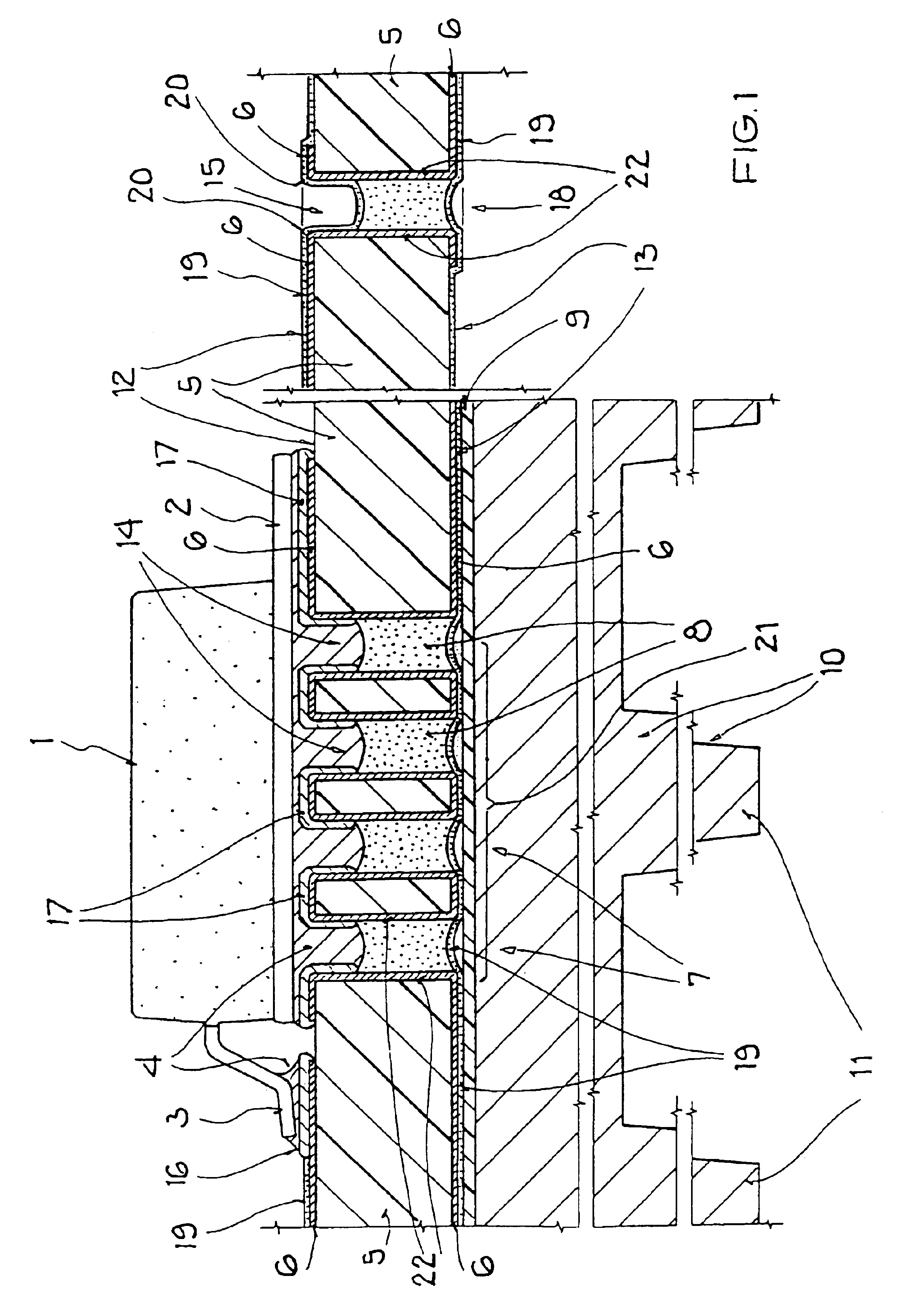
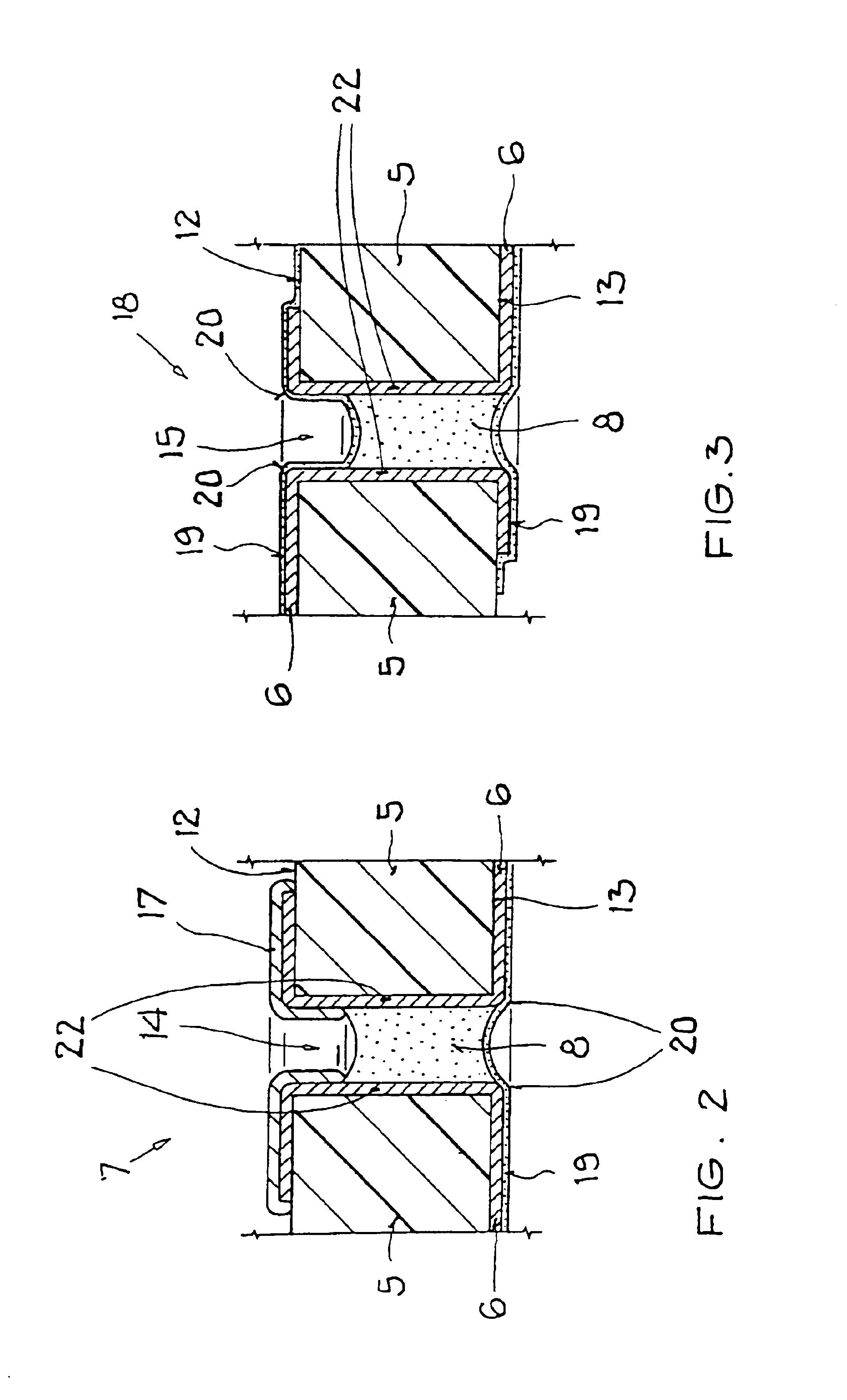
[0021]The circuit arrangement of the electronic package arranged on the top side 12, for example of a printed circuit board formed as a carrier body 5, comprises in addition to further active and passive electronic components also at least one power component 1, the connector contacts 3 of which are to be contacted through the connector pad 16 with the printed circuit structure applied to the printed circuit board 5. Furthermore, electrical vias 18 as well as thermal vias 7 are provided to pass from the top side 12 of the printed circuit board 5 to the bottom side 13 of the printed circuit board 5. The vias 7, 18 may, for example have a diameter in the range of 0.2 mm to 1.2 mm. Bores constructed as lead-throughs are introduced into the printed circuit board 5 for forming the vias 7 and 18. The wall surfaces 22 of the vias are completely and over the entire surface covered with a first metallization layer 6, for example of copper, for realizing the printed circuit structure. Followi...


PUM


Abstract

Electronic packages are produced as follows. Vias in a support body are closed with a highly viscous screen printing material following application of a first metallizing layer forming a base metallization on the support body and in the lead-throughs for the vias. A low viscosity passivating layer, which has been applied on the entire surface of the top and bottom sides of the support body, is selectively removed from certain areas of the top side. A second metailizing layer forming the final metallization of a low-melting point material is applied to the first metallization layer in the areas from which the passivating layer was removed. Electronic components of the circuit arrangement are applied on the top side of the support body and contacted by a soldering process.

Description

CROSS-REFERENCE TO RELATED APPLICATION[0001]This application relates to U.S. application Ser. No. 09 / 914,932, PCT filed: Mar. 1, 2000, now U.S. Pat. No. 6,820,798, issued Nov. 23, 2004, for “Method for Producing Circuit Arrangements”.FIELD OF THE INVENTION[0002]An electronic package is formed to include a circuit arrangement and at least one electronic component on a support or substrate.BACKGROUND OF THE INVENTION[0003]Electronic packages are used in many application areas of electrical engineering. These electronic packages comprise circuit arrangements with electronic components. A high power dissipation occurs during operation. This is particularly the case in electronic packages including power components such as power modules for the control of electronic components or of further packages. The components of the circuit arrangement of the electronic package are applied to a suitable support body, for example, power components that are frequently surface mountable are used in po...

Claims


Application Information

Patent Timeline
IPC IPC(8): H05K3/00H05K1/02H05K3/28H05K3/42H05K1/11H05K3/34H05K3/12
CPCH05K1/0206H05K3/0094H05K1/112H05K3/1216H05K3/28H05K3/341H05K3/3452H05K3/42H05K2201/0195H05K2201/066H05K2201/0959H05K2201/10166H05K2203/025H05K2203/044H05K2203/0455H05K2203/0588
Inventor HEINZ, HELMUTNEHMEIER, FRIEDRICHSCHUCH, BERNHARDTRAGESER, HUBERT
Owner CONTI TEMIC MICROELECTRONIC GMBH
Why Eureka
Try Eureka