
Semiconductor device and method of manufacturing the same

a technology of magnetic field and semiconductor, applied in the direction of magnetic field devices, transistors, electrical equipment, etc., can solve the problems of reducing the cells per unit bit line, generating single bit failures, and difficult to form a small contact hole using conventional methods, so as to reduce the shoulder margin of a bit line and the effect of bit line loading capacitance reduction

Active Publication Date: 2005-07-12
SAMSUNG ELECTRONICS CO LTD
View PDF4 Cites 13 Cited by
  • Summary
  • Abstract
  • Description
  • Claims
  • Application Information

AI Technical Summary

Benefits of technology

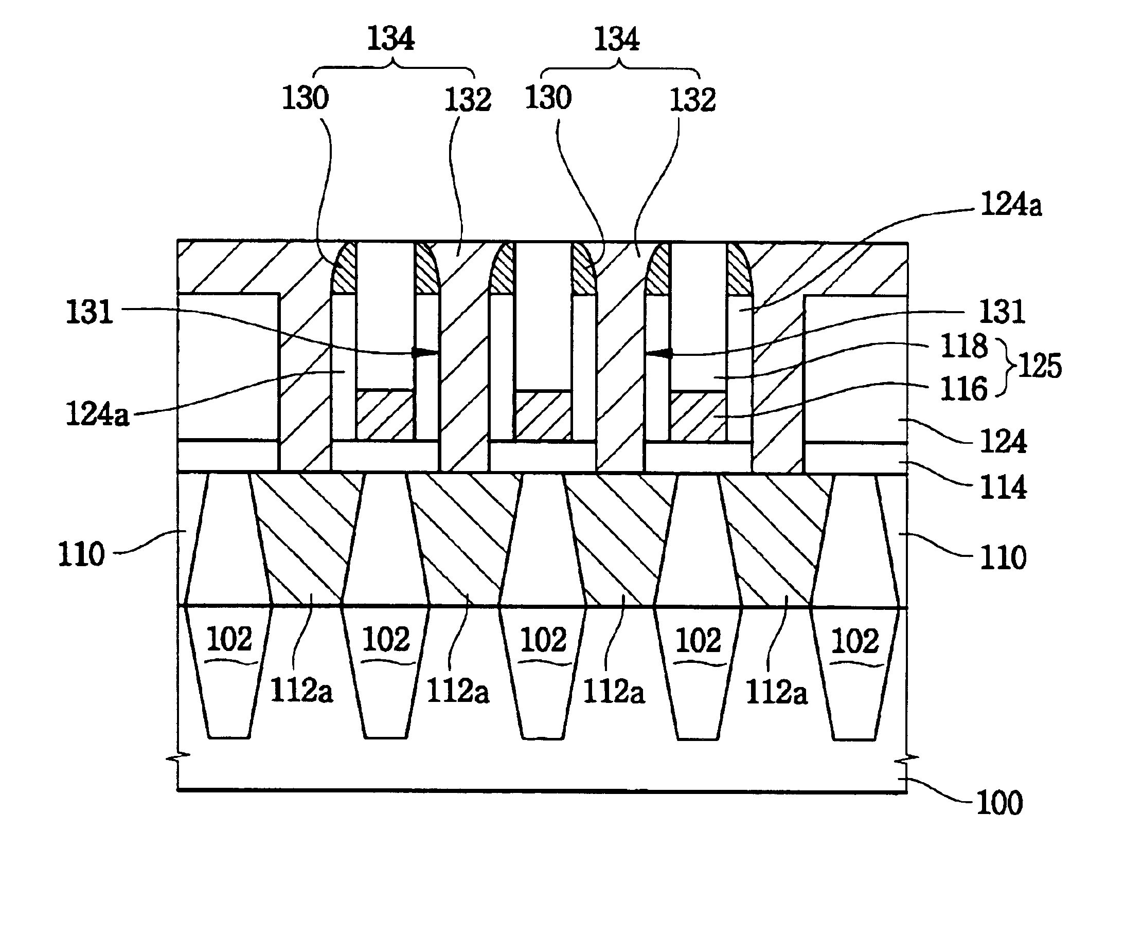
[0027]Embodiments of the invention provide a semiconductor device wherein a gap formed between bit lines is effectively filled without generations of voids, a shoulder margin of a bit line is augmented, and a bit line loading capacitance is reduced.
[0028]Embodiments of the invention provide a method of manufacturing a semiconductor device that effectively fills a gap generated between bit lines without voids, increases the shoulder margin of the bit line, and reduces the bit line loading capacitance.

Problems solved by technology

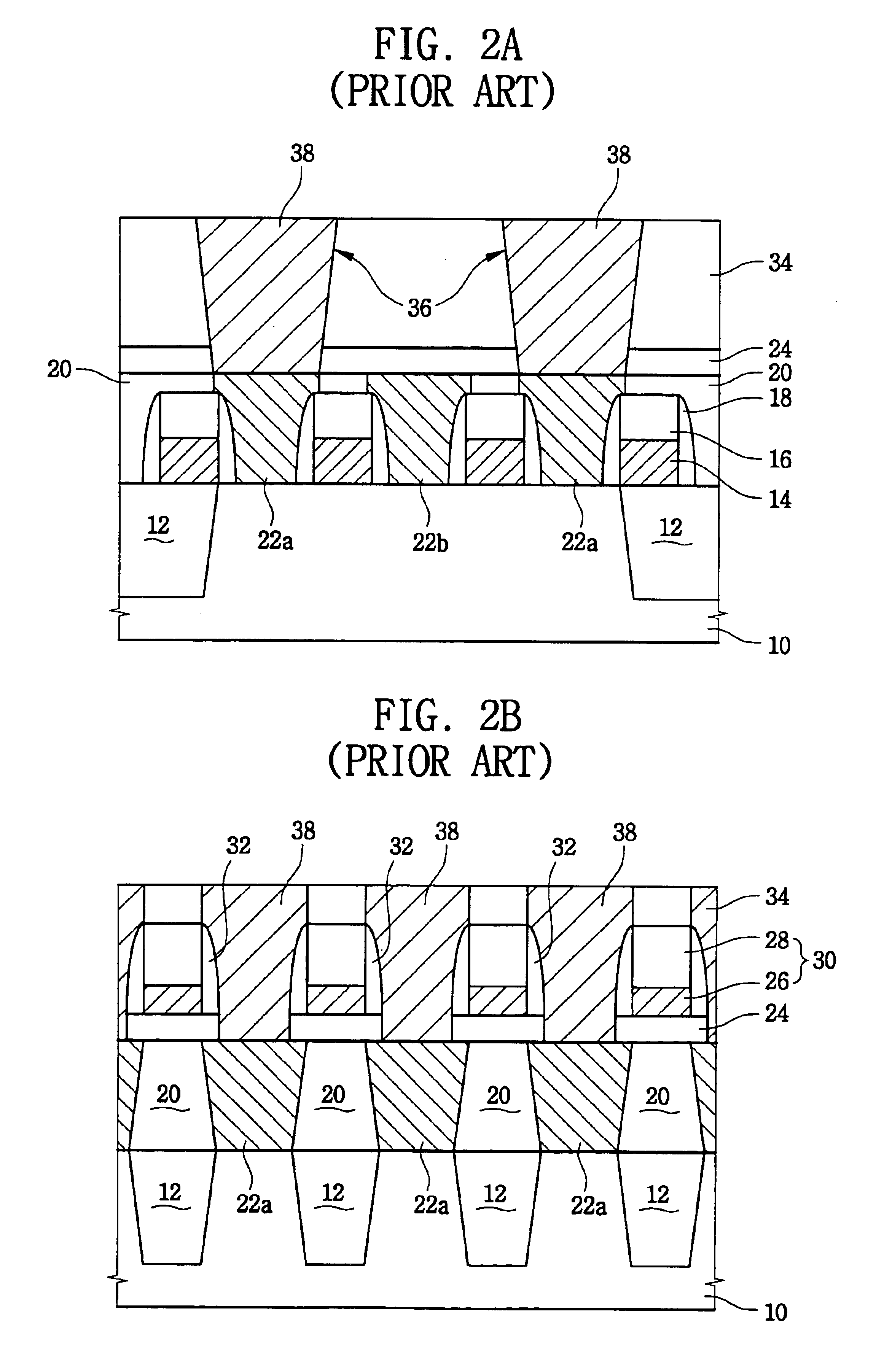
As a result, formation of a small contact hole becomes very difficult using conventional methods.
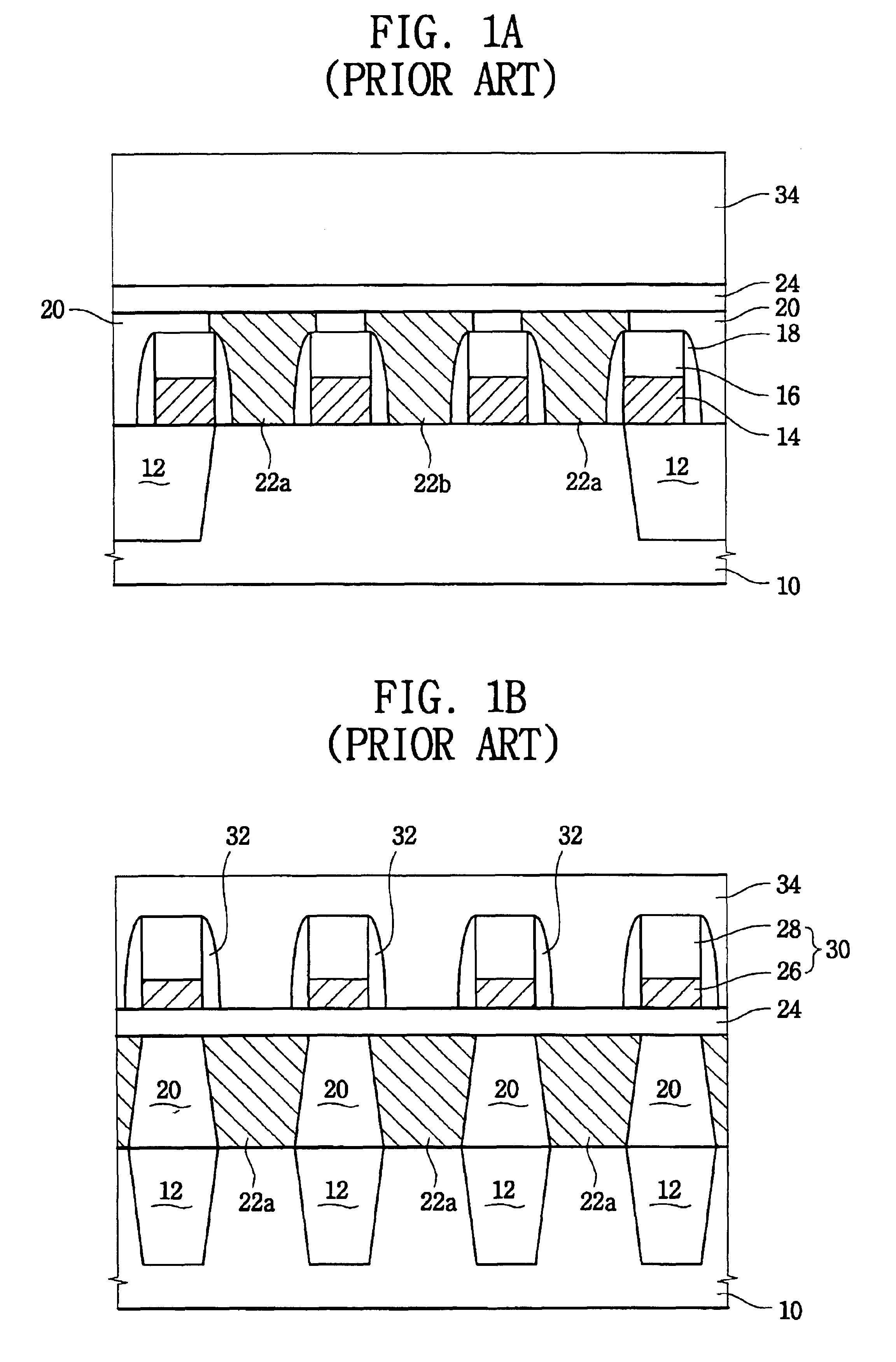
Furthermore, since the bit line mask layer 28 may be damaged during the etching processes of forming the bit line spacers 32 and forming the storage node contact holes 36, the bit lines 30 are electrically short-circuited relative to the storage node contact pads 38, thereby generating single bit failures.
Thus, the number of the bit lines constituting a cell array of the DRAM device should be reduced considering the bit line loading capacitance, which results in a reduction of cells per unit bit line and deteriorates chip efficiency.
However, the reduction of the thickness of a bit line mask layer may be limited to decrease the gap-fill margin of an interlayer dielectric layer.
Additionally, there is scarcely any shoulder margin of the bit line, which results in a generation of an electrical short-circuit between the bit line and a storage node contact pad.

Method used


Image

  • Semiconductor device and method of manufacturing the same
  • Semiconductor device and method of manufacturing the same
  • Semiconductor device and method of manufacturing the same

Examples


Embodiment Construction

[0034]It should be understood that exemplary embodiments of the invention described below may be varied modified in many different ways without departing from the inventive principles disclosed herein, and the scope of the invention is therefore not limited to these particular following embodiments. Rather, these embodiments are provided so that this disclosure will be thorough and complete, and will fully convey the concept of the invention to those skilled in the art by way of example and not of limitation.

[0035]Hereinafter embodiments of the invention will be explained with reference to the accompanying drawings. In the drawings, like reference numerals identify similar or identical elements.

[0036]FIGS. 3A-3C, 4A-4D, 5A-5D, 6A-6D, 7A-7D, 8A-8D, and 9A-9D are plan diagrams and cross-sectional diagrams illustrating a method of manufacturing a DRAM device according to an embodiment of the invention.

[0037]FIG. 3A is a plan diagram of a semiconductor substrate 100 on which word lines ...


PUM

PropertyMeasurementUnit
sizeaaaaaaaaaa
aspect ratioaaaaaaaaaa
dielectric constantaaaaaaaaaa

Abstract

Bit lines having first conductive patterns and bit line mask patterns are formed on a first insulating layer between capacitor contact regions of a substrate. An oxide second insulating layer is formed on the bit lines and contact patterns are formed to open storage node contact hole regions corresponding to portions of the second insulating layer. First spacers are formed on sidewalls of the etched portions. The second and first insulating layers are etched to form storage node contact holes exposing the capacitor contact regions. Simultaneously, second spacers of the second insulating layer are formed beneath the first spacers. A second conductive layer fills the storage node contact holes to form storage node contact pads. A loss of the bit line mask pattern decreases due to the reduced thickness of the bit line mask pattern and a bit line loading capacitance decreases due to the second spacers.

Description

CROSS REFERENCE TO RELATED APPLICATIONS[0001]This application claims priority from Korean Patent Application No. 2003-11310, filed on Feb. 24, 2003, the contents of which are hereby incorporated by reference in their entirety.BACKGROUND OF THE INVENTION[0002]1. Field of the Invention[0003]This disclosure relates to a semiconductor device and, more particularly, to a dynamic random access memory (DRAM) and a method of manufacturing the same.[0004]2. Description of the Related Art[0005]As technologies for manufacturing semiconductor devices have been developed and applications for memory devices have been expanded, memory devices having large capacities have been required. In particular, an integration density of a DRAM device wherein a memory cell is composed of one capacitor and one transistor has been remarkably improved.[0006]Accordingly, as an integration density of a semiconductor device increases, a size of the contact hole connecting one element to another element or one layer...

Claims


Application Information

Patent Timeline
Patent Type & Authority Patents(United States)
IPC IPC(8): H01L29/76H01L21/4763H01L21/70H01L21/02H01L21/768H01L21/8242H01L27/108H01L29/66H10B12/00
CPCH01L27/10888H01L27/10855H01L27/0207H01L27/10814H01L27/10885H10B12/315H10B12/485H10B12/0335H10B12/482H10B12/00
Inventor LEE, JAE-GOOYUN, CHEOL-JU
Owner SAMSUNG ELECTRONICS CO LTD
Learn More