
Semiconductor device and manufacturing method therefor

a technology of semiconductors and semiconductors, applied in the direction of semiconductor devices, electrical devices, transistors, etc., can solve the problems of increasing leakage current, reducing film thickness, and difficult to obtain an equivalent oxide thickness of 1.5 nm or less, and achieve the effect of reducing pressur

Active Publication Date: 2005-06-21
MICROSOFT TECH LICENSING LLC
View PDF17 Cites 39 Cited by
  • Summary
  • Abstract
  • Description
  • Claims
  • Application Information

AI Technical Summary

Benefits of technology

The present invention provides a semiconductor device and a manufacturing method with good interfacial characteristics between the insulating film and silicon substrate. The method forms a high dielectric constant insulating film on top of a first insulating film, which is either a silicon oxide film with low suboxide content or a silicon nitride film with low oxygen content. The surface of the silicon substrate is treated with a non-oxidizing gas under reduced pressure before the first insulating film is formed. The technical effects of the invention include improved performance and reliability of semiconductor devices.

Problems solved by technology

However, reducing the film thickness of gate insulating films of such materials (considerably) increases the leakage current.
However, when a metal oxide film or a metal silicate film is directly formed on a silicon substrate, the surface of the silicon substrate is oxidized due to heat treatment during or after the film forming process, resulting in formation of a silicon oxide film whose film thickness is as large as 1.5 nm or more.
Therefore, it has been difficult to obtain an equivalent oxide thickness of 1.5 nm or less.
Furthermore, there is another problem with this type of silicon oxide film.
This leads to an increased leakage current.
However, since the moisture within the processing chamber is difficult to control, it is considered that it is difficult to produce a semiconductor device including a metal oxide film or a metal silicate film by the above method.
However, it is difficult to hydrogen-terminate all silicon atoms present in the surface of the silicon substrate.
However, since they form one to three atomic layers of silicon oxide (film) and nitride them, the same problem as that described above in connection with formation of a silicon oxide film arises.
However, the CVD technique uses an oxidizing gas such as water molecules, oxygen molecules, oxygen radicals, or ozone, making it difficult to reduce the increase in the film thickness of the underlying film.

Method used


Image

  • Semiconductor device and manufacturing method therefor
  • Semiconductor device and manufacturing method therefor
  • Semiconductor device and manufacturing method therefor

Examples


first embodiment

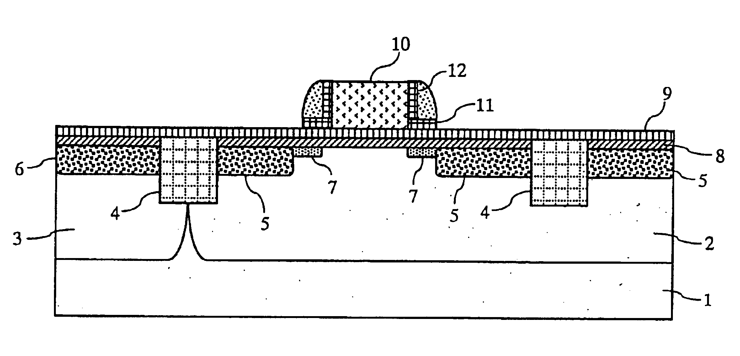
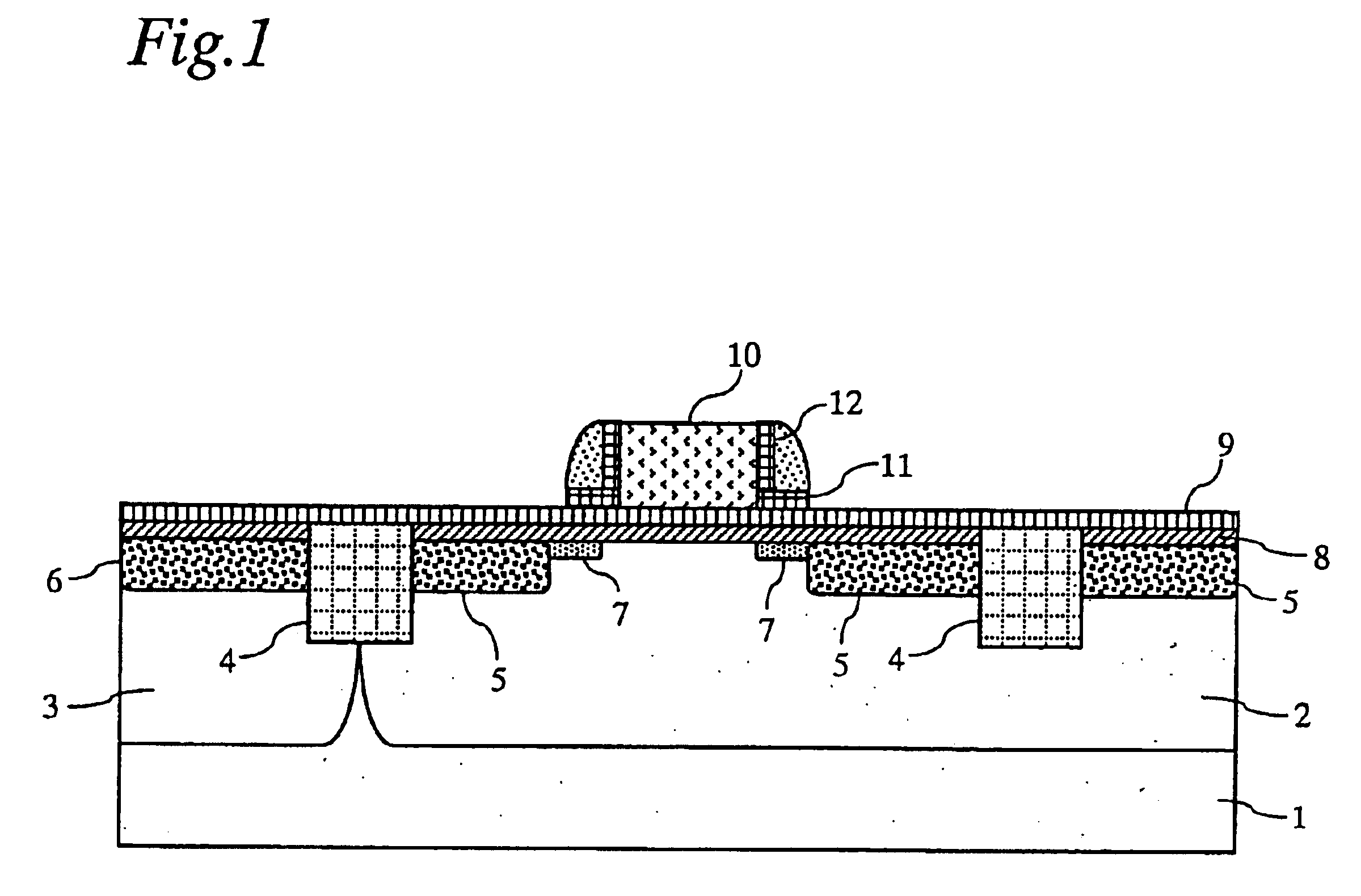
[0029]FIG. 1 is a cross-sectional view of a semiconductor device according to a first embodiment of the present invention.

[0030]As shown in FIG. 1, in a silicon substrate 1 are formed an N type diffusion layer 2, a P type diffusion layer 3, device separation regions 4, a P type source / drain diffusion layer 5, an N type source / drain diffusion layer 6, and P type extension regions 7. Furthermore, as a first insulating film, a silicon oxide film 8 is formed on the entire surface of the silicon substrate 1 except for the device separation regions 4. According to the present embodiment, the film thickness of the silicon oxide film 8 is set to 1 nm or less, and its suboxide content is set to 30% or less.

[0031]Further, a hafnium silicate film 9 is formed on the silicon oxide film 8 as a second insulating film, and a gate electrode 10 is formed on the hafnium silicate film 9. Still further, a silicon oxide film 11 and a silicon nitride film 12 are formed on the sidewalls of the gate electro...

second embodiment

[0078]A second embodiment of the present invention is characterized in that a silicon oxynitride film is used as a first insulating film.

[0079]FIG. 4 is a cross-sectional view of a semiconductor device according to the present embodiment.

[0080]As shown in FIG. 4, in a silicon substrate 1 are formed an N type diffusion layer 2, a P type diffusion layer 3, device separation regions 4, a P type source / drain diffusion layer 5, an N type source / drain diffusion layer 6, and P type extension regions 7. Furthermore, a nickel silicide layer 21 is formed on the P type source / drain diffusion layer 5 and the N type source / drain diffusion layer 6. It should be noted that another metal silicide layer such as a cobalt silicide layer or a titanium silicide layer may be formed instead of the nickel silicide layer 21.

[0081]Also, a silicon oxynitride film 22 is formed on the silicon substrate 1 as a first insulating film. Furthermore, a hafnium silicate film 23 is formed on the silicon oxynitride film...

third embodiment

[0118]FIG. 6 is a cross-sectional view of a semiconductor device according to a third embodiment of the present invention. The semiconductor device has a structure similar to that of the semiconductor device of the second embodiment shown in FIG. 4. However, the third embodiment is characterized in that a silicon nitride film is used as a first insulating film.

[0119]As shown in FIG. 6, in a silicon substrate 1 are formed an N type diffusion layer 2, a P type diffusion layer 3, device separation regions 4, a P type source / drain diffusion layer 5, an N type source / drain diffusion layer 6, P type extension regions 7, and N type extension regions 26. Furthermore, a nickel silicide layer 21 is formed on the P type source / drain diffusion layer 5 and the N type source / drain diffusion layer 6. It should be noted that another metal silicide layer such as a cobalt silicide layer or a titanium silicide layer may be formed instead of the nickel silicide layer 21.

[0120]Also, a silicon nitride fi...


PUM

PropertyMeasurementUnit
thicknessaaaaaaaaaa
thicknessaaaaaaaaaa
thicknessaaaaaaaaaa

Abstract

A semiconductor device includes a first insulating film on a silicon substrate and a second insulating film on the first insulating film. The first insulating film is a silicon oxide film having a thickness of 1 nm or less and a suboxide content of 30% or less. The second insulating film is a high dielectric constant insulating film.

Description

BACKGROUND OF THE INVENTION[0001]1. Field of the Invention[0002]The present invention relates to a semiconductor device and a manufacturing method therefor, and more particularly to a semiconductor device including a high dielectric constant insulating film and a manufacturing method therefor.[0003]2. Background Art[0004]In recent years, the integration density of semiconductor integrated circuit devices has considerably increased. As such, devices such as transistors for MOS (Metal Oxide Semiconductor) devices, for example, have been miniaturized and enhanced in performance. Especially, the gate insulating films, which are a component of the MOS structure, have become thinner and thinner to accommodate the miniaturization, higher-speed operation, and lower-voltage operation of the transistors.[0005]Conventionally, silicon oxide films and silicon oxynitride films have been used for gate insulating films. However, reducing the film thickness of gate insulating films of such materials...

Claims


Application Information

Patent Timeline
Patent Type & Authority Patents(United States)
IPC IPC(8): H01L21/02H01L21/70H01L21/28H01L29/51H01L29/40H01L21/8238H01L27/092H01L21/316H01L21/318H01L21/336H01L29/78
CPCH01L21/28185H01L21/28194H01L21/28202H01L29/518H01L29/513H01L29/517H01L21/823857H01L21/18
Inventor AOYAMA, TOMONORI
Owner MICROSOFT TECH LICENSING LLC
Learn More