Silicon oxide film evaluation method and semiconductor device fabrication method

Inactive Publication Date: 2005-05-10
LAPIS SEMICON CO LTD
View PDF8 Cites 3 Cited by
  • Summary
  • Abstract
  • Description
  • Claims
  • Application Information

AI Technical Summary

Benefits of technology

[0009]An object of the present invention is to provide a simple and quick method of evaluating and controlling the degradation of power characteristics of a FET having a silicon oxide interlayer film during the film fabrication process.
[0012]The invention also provides a method of fabricating a semiconductor device including a FET having a silicon oxide interlayer film formed on a compound semiconductor substrate. The method includes analyzing the silicon oxide interlayer film by FT-IR spectroscopy and estimating the quantity of silicon-silicon bonds as described above, determining a fabrication process condition for forming the silicon oxide film so as to reduce the quantity of silicon-silicon bonds, and forming the interlayer silicon oxide film according to this fabrication process condition. The estimated quantity of silicon-silicon bonds provides an index of expected power performance degradation during operation of the FET, so fabricating the semiconductor device under a condition that reduces the estimated quantity of silicon-silicon bonds reduces the expected power degradation, without the need for actual measurement of the power degradation.

Problems solved by technology

When a high-output compound semiconductor FET is driven for an extended period of time, its power output degrades due to the effect of electrons trapped in the interlayer film, or between the compound semiconductor substrate and the interlayer film.
Reference 1 deals with mitigation of the degradation of power characteristics of a high-output compound semiconductor FET having a silicon nitride film, but does not address the degradation of power characteristics of a high-output FET having a silicon oxide film formed on a compound semiconductor substrate.
This method is not suitable for use during mass production of semiconductor devices.

Method used


Image

  • Silicon oxide film evaluation method and semiconductor device fabrication method
  • Silicon oxide film evaluation method and semiconductor device fabrication method
  • Silicon oxide film evaluation method and semiconductor device fabrication method

Examples


example 1

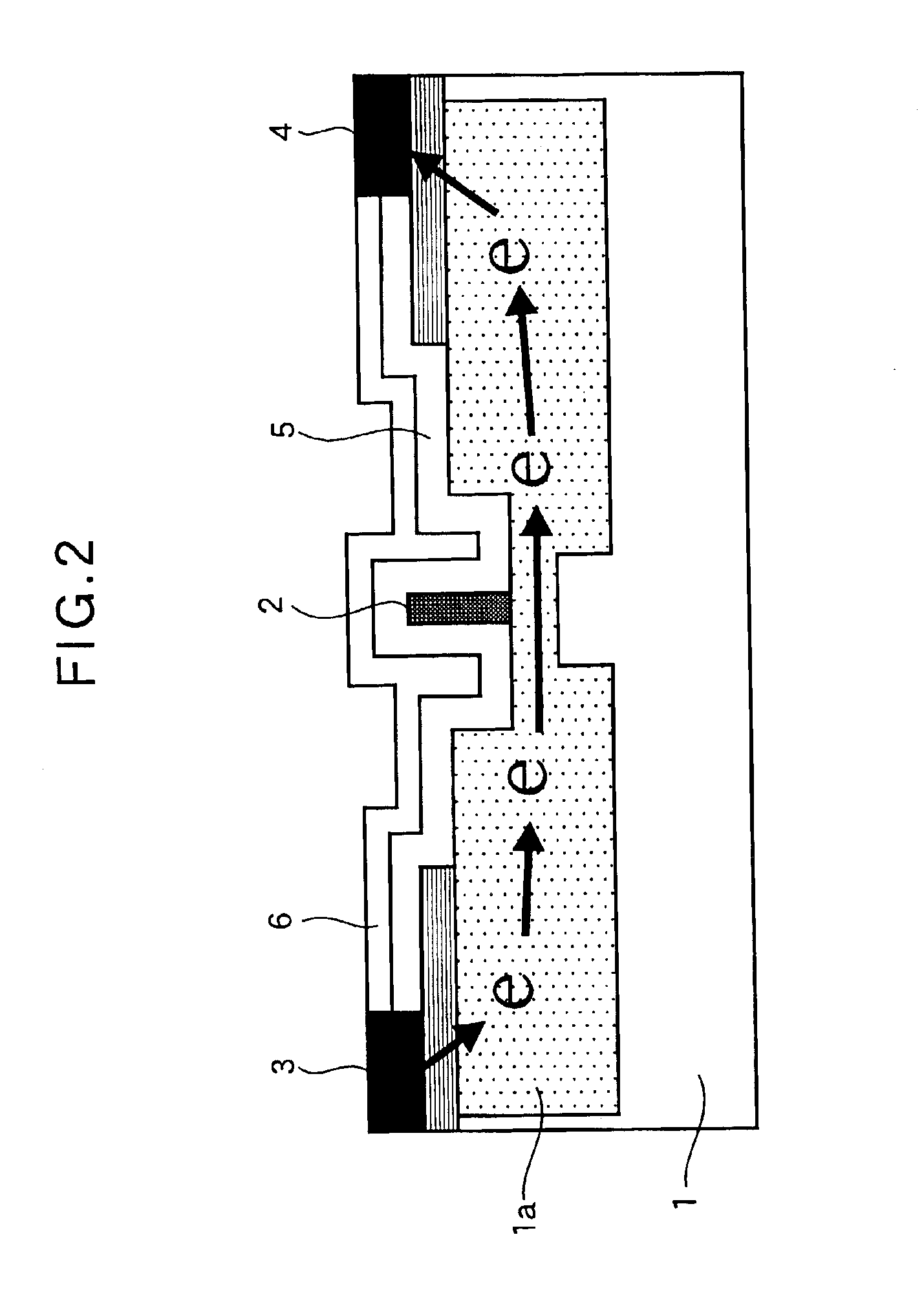
[0054]A silicon oxide film deposited on a dummy GaAs wafer substrate is analyzed by using FT-IR spectroscopy. From the peak at wave number 810 cm−1 in the FT-IR spectrum, fabrication process conditions for forming the silicon oxide film are determined so as to reduce the quantity of Si—Si bonds, which is used as an index of the expected FET power characteristic degradation. A silicon oxide interlayer film is formed according to these fabrication process conditions on a GaAs wafer substrate product used for the fabrication of a high-output FET.

example 2

[0055]The silicon oxide interlayer film is formed on a GaAs wafer substrate product used for the fabrication of a high-output FET. This silicon oxide interlayer film is analyzed by using, for example, a micro-infrared spectroscopy technique capable of measuring reflectance. From the peak at wave number 810 cm−1 in the FT-IR spectrum, the quantity of Si—Si bonds is estimated as an index of expected FET power characteristic degradation. The quality of the interlayer film is determined from the estimated quantity of Si—Si bonds.

example 3

[0056]The fabrication process conditions are determined by using FT-IR spectroscopy as described in Example 1, and the interlayer film is evaluated as described in Example 2.

[0057]As described above, the present invention enables the degradation of power characteristics of a FET to be evaluated and controlled by a simple method during the silicon oxide interlayer film fabrication process. A drive test over an extended period of time is not required, so degradation can be evaluated quickly.

[0058]The embodiment described above has dealt with a high-output FET on a GaAs substrate having a silicon oxide film, but the invention can also be applied to a high-output FET on another compound substrate, such as an indium-phosphorus substrate or a gallium-nitride substrate, having a silicon oxide interlayer film.

[0059]As described above, the invention has the effect of evaluating and controlling the degradation of power characteristics of an FET simply and quickly during the silicon oxide inte...


PUM


Abstract

A silicon oxide film formed on a compound semiconductor substrate is evaluated by estimating the quantity of silicon-silicon bonds operating as electron traps in the silicon oxide film from a peak with a wave number of 880 / centimeter in the Fourier-transform infrared spectrum of the silicon oxide film. This peak, which is an indicator of silicon-silicon stretching vibration, provides an index of expected power performance degradation during operation of field-effect transistors incorporating the silicon oxide film as an interlayer. Power degradation can be reduced by fabricating the semiconductor device under conditions that reduce the estimated quantity of silicon-silicon bonds, without the need to measure the power degradation.

Description

BACKGROUND OF THE INVENTION[0001]1. Field of the Invention[0002]The present invention relates to a method of fabricating a semiconductor device in which a field-effect transistor (FET) having a silicon oxide interlayer film is formed on a compound semiconductor substrate, and more particularly to a method of evaluating the interlayer film in order to control the degradation of FET power characteristics due to electron trapping.[0003]2. Description of the Related Art[0004]When a high-output compound semiconductor FET is driven for an extended period of time, its power output degrades due to the effect of electrons trapped in the interlayer film, or between the compound semiconductor substrate and the interlayer film. A description of this effect is given in “Relationship between gate lag, power drift, and power slump of pseudomorphic high electron mobility transistors,” Solid-State Electronics 43 (1999), pp. 1325-1331 (hereinafter, Reference 1).[0005]One method of assessing the degra...

Claims


Application Information

Patent Timeline
IPC IPC(8): G01N21/31G01N21/35G01N21/84H01L21/66G01N21/3563G01N21/00H01L29/80
CPCG01N21/3563G01N21/8422G01N2021/3595H01L22/12
Inventor OKAJIMA, TAKEHIKO
Owner LAPIS SEMICON CO LTD
Why Eureka
Try Eureka