Eureka AIR delivers breakthrough ideas for toughest innovation challenges, trusted by R&D personnel around the world.

Multimode system for calibrating a data strobe delay for a memory read operation

a multi-mode system and data strobe technology, applied in the field of multi-mode systems for calibrating data strobe delays for memory read operations, can solve the problems of not solving the problem of timing a dqs, requiring a certain amount of setup time, and capturing purious data, so as to achieve flexibility in its use and application.

Inactive Publication Date: 2005-05-03
ADVANCED MICRO DEVICES INC
View PDF24 Cites 112 Cited by
  • Summary
  • Abstract
  • Description
  • Claims
  • Application Information

AI Technical Summary

Benefits of technology

The present invention is a system and method for calibrating the timing of data strobes in a processor-based system. It includes a programmable delay line (PDL) with delay buffer elements that can be selected by a user or autocalibration subsystem to adjust the delay time based on temperature or voltage variations. The system allows for real-time calibration triggered by external factors or user interaction. The technical effect of the invention is to ensure accurate and flexible timing of data strobes in a processor-based system.

Problems solved by technology

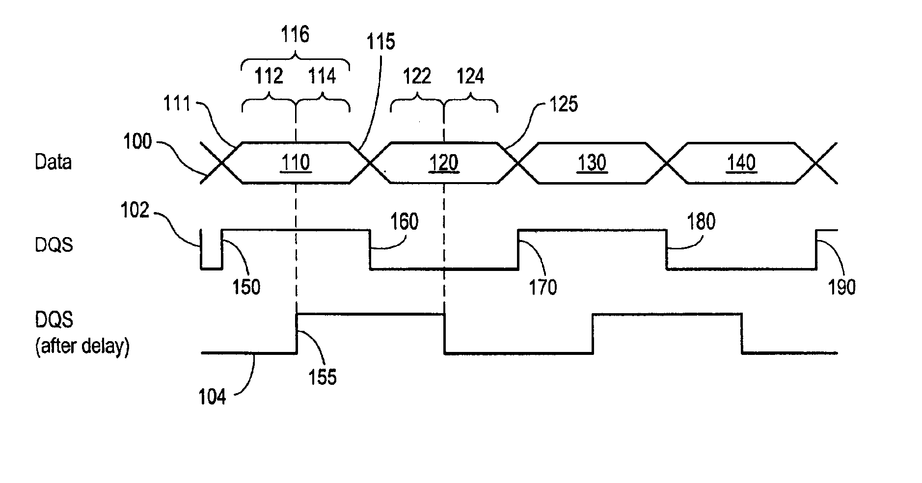
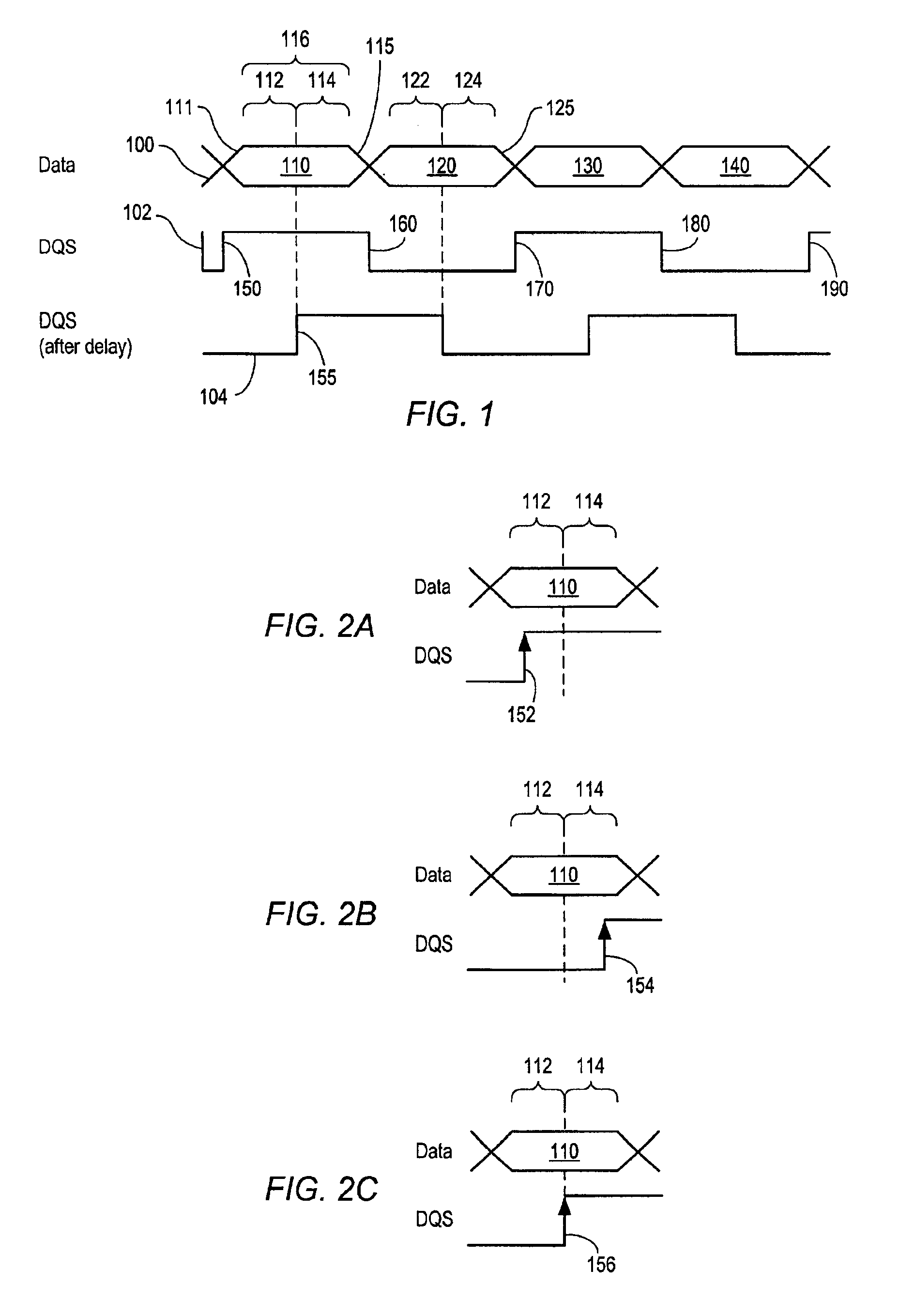
When this occurs, spurious data can be captured, since the receiving device may not have had time to stabilize.
However, care must be taken that the DQS is not delayed too much, or it might occur at or near the end of the hold period 114, as in FIG. 2B, with the risk of attempting to capture the data during the tail transition time, again leading to erroneous data.
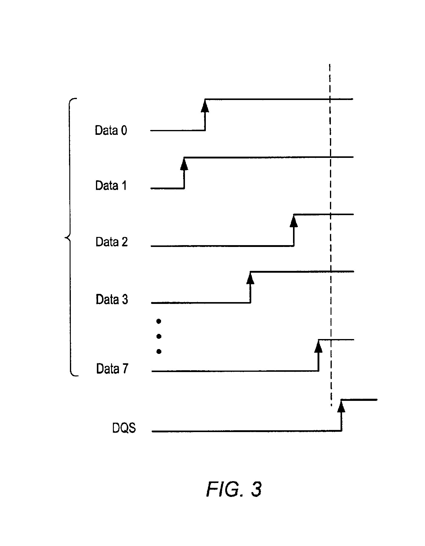
Not only does the setup take a certain amount of time, but the bits that make up a data word may take different paths from a memory device (e.g. a DIMM) through the system (even though they are all on the same bus), resulting in misalignment—i.e., different arrival times at the requesting device.
Such mechanisms will keep the system clock's frequency within the capture and tracking ranges of the PLL, but this does not solve the problem of timing a DQS strobe as discussed above.
A PLL is inappropriate to time a DQS strobe, in part because a PLL requires a constant clock signal (unlike a DQS strobe, which can stop between data transfers); and additionally, because a PLL is designed to minimize variations in signal frequencies (and hence timing differences), whereas a DQS strobe must be affirmatively delayed for correct timing with the data signals.
A problem with attempting to specify a fixed delay period is that as the chip or circuit warms up under load, the delay period will lengthen, while the data window remains within tight parameters, while the “fixed” delay period typically may vary to a greater degree.
Although tight circuit board specifications can alleviate this—e.g. by careful routing and linking the data lines as closely as possible to the clock—the problem of DQS strobe timing persists.

Method used


Image

  • Multimode system for calibrating a data strobe delay for a memory read operation
  • Multimode system for calibrating a data strobe delay for a memory read operation
  • Multimode system for calibrating a data strobe delay for a memory read operation

Examples


Embodiment Construction

[0034]FIG. 4 is a block diagram of a processor-based system 200, such as a workstation or server, incorporating features implementing an embodiment of the present invention. The system 200 operates under control of at least one microprocessor 210, a display 220 and one or more user interface devices 230 (such as keyboard, mouse, track ball, etc.).

[0035]The processor 210 is connected to a local device control circuitry 240 (also referred to as a “host bridge”), which includes circuitry that controls data and command exchanges with local devices such as the display 220 via an accelerated graphics processor (AGP) 250 and memory 260, which may in a typical system will include multiple DIMMs and / or other suitable memory modules or media.

[0036]The local device control circuitry 240 is connected to a peripheral device control circuit 270 via a bus such as PCI bus 280.

[0037]The local device control circuitry 340 may in many respects include conventional or known circuitry (with the addition...


PUM


Abstract

A system for coordinating the timing of a data strobe with data supplied by a memory module to the memory controller read data FIFO of a processor-based system, providing multiple calibration modes. A calibration PDL (programmable delay line) is used to reiteratively test the time taken for a test data strobe to traverse a portion of the memory controller circuit, and to generate a calibration value based upon the time taken. The calibration procedure may be initiated in any one of several modes, including: according to a predetermined schedule; implemented in software; in response to changes in environmental factors such as temperature or voltages sampled at one or more locations; in response to a software-driven trigger; or in response to a user-initiated trigger, communicated to a system of the invention either by input via a user interface to the processor-based system or by a software command.

Description

BACKGROUND OF THE INVENTION[0001]The present invention relates to the positioning of a data strobe within a data valid window in a processor-based system that executes data read and write operations by accessing memory modules such as DIMMs (double in-line memory modules). In particular, the system and method described herein are adapted to accommodate the stringent requirements presented by DDR (double-data read) systems, which clock memory data at both the positive and negative edges of a data strobe (referred to as DQS) signal, and which are becoming more common in high-end computer systems.[0002]DDR devices use a source-synchronous clocking mechanism (the DQS strobe) to transfer data between the DDR device and the memory controller. During a read access, the DDR device provides read data substantially aligned with the DQS data strobe, and the memory controller, such as a DDR SDRAM controller, delays the DQS data strobe by an amount determined to accommodate the appropriate setup...

Claims


Application Information

Patent Timeline
Patent Type & Authority Patents(United States)
IPC IPC(8): G06F1/06G11C7/10H04L7/00
CPCG11C7/1051G11C7/1066G11C7/1072H04L7/0037H04L7/0004G11C7/222G11C2207/2254H04L7/0008
Inventor MAGRO, JAMES R.LOYER, BRUCE A.MEHTA, PRATIK M.
Owner ADVANCED MICRO DEVICES INC
Why Eureka
Eureka Blog
Learn More