CDM ESD protection design using deep N-well structure

a protection device and cdm technology, applied in the direction of emergency protection circuit arrangements for limiting excess voltage/current, emergency protection circuit arrangements, etc., can solve the problems of esd protection circuits that cannot cope with cdm esd stress, esd protection circuits that endure high hmb or mm esd stress, etc., to reduce noise coupling, maintain circuit performance, and reduce leakage current

Inactive Publication Date: 2005-04-26
TAIWAN SEMICON MFG CO LTD
View PDF11 Cites 44 Cited by
  • Summary
  • Abstract
  • Description
  • Claims
  • Application Information

AI Technical Summary

Benefits of technology

[0021]The advantage of the present invention is that by using an isolating region, most of the significant electrostatic charges stored in the substrate are discharged through the ESD clamp circuit, rather than through the functioning component, to the pad. Additionally, the electrostatic charges in the first well is too few to damage the gate oxide of the functioning component.
[0022]As technology of deep sub-micron CMOS advances, IC products often have high-integration circuit blocks, such as embedded dynamic random-access-memory (DRAM)or mixed-mode circuits (analog circuit blocks). In order to maintain the circuit performance of the embedded DRAM or mixed-mode (analogue) circuits, or to reduce noise coupling through common p-type substrate, a deep N-well structure is often added into the CMOS processes to meet the required circuit specifications. Especially, the memory cells of the embedded DRAM are placed in a stand-alone p-well region which is isolated from the common p-type substrate by a deep N-well structure. The common p-type substrate is generally biased at 0V (ground) for most of the applications. With the addition of the deep N-well structure, the stand-alone p-well region can be biased with a negative voltage level to reduce the leakage current of the switch MOS in the memory cell. In the mixed-mode circuit, the high-resolution circuit performance of the analog circuits is easily disturbed by noises generated from the digital logic blocks. With the additional deep N-well structure in the CMOS technology, the NMOS devices of analog circuits are placed at the isolated p-well region, which is isolated from the noisy common p-substrate. Therefore, the deep N-well structure has been generally included into the sub-micron CMOS process to support the IC design for high-integration applications.

Problems solved by technology

The substrate is filled with a substantial amount of electrostatic charges which transiently cause overstress and breakdown of the gate oxide of the input buffers.
Conventional ESD protection circuits endure high HMB or MM ESD stress, but cannot cope with this CDM ESD stress.
Such a design, on the other hand, produces IC more susceptible to the latch-up effect.
However, this will increase the layout complexity of the circuit around the pad.

Method used


Image

  • CDM ESD protection design using deep N-well structure
  • CDM ESD protection design using deep N-well structure
  • CDM ESD protection design using deep N-well structure

Examples


Embodiment Construction

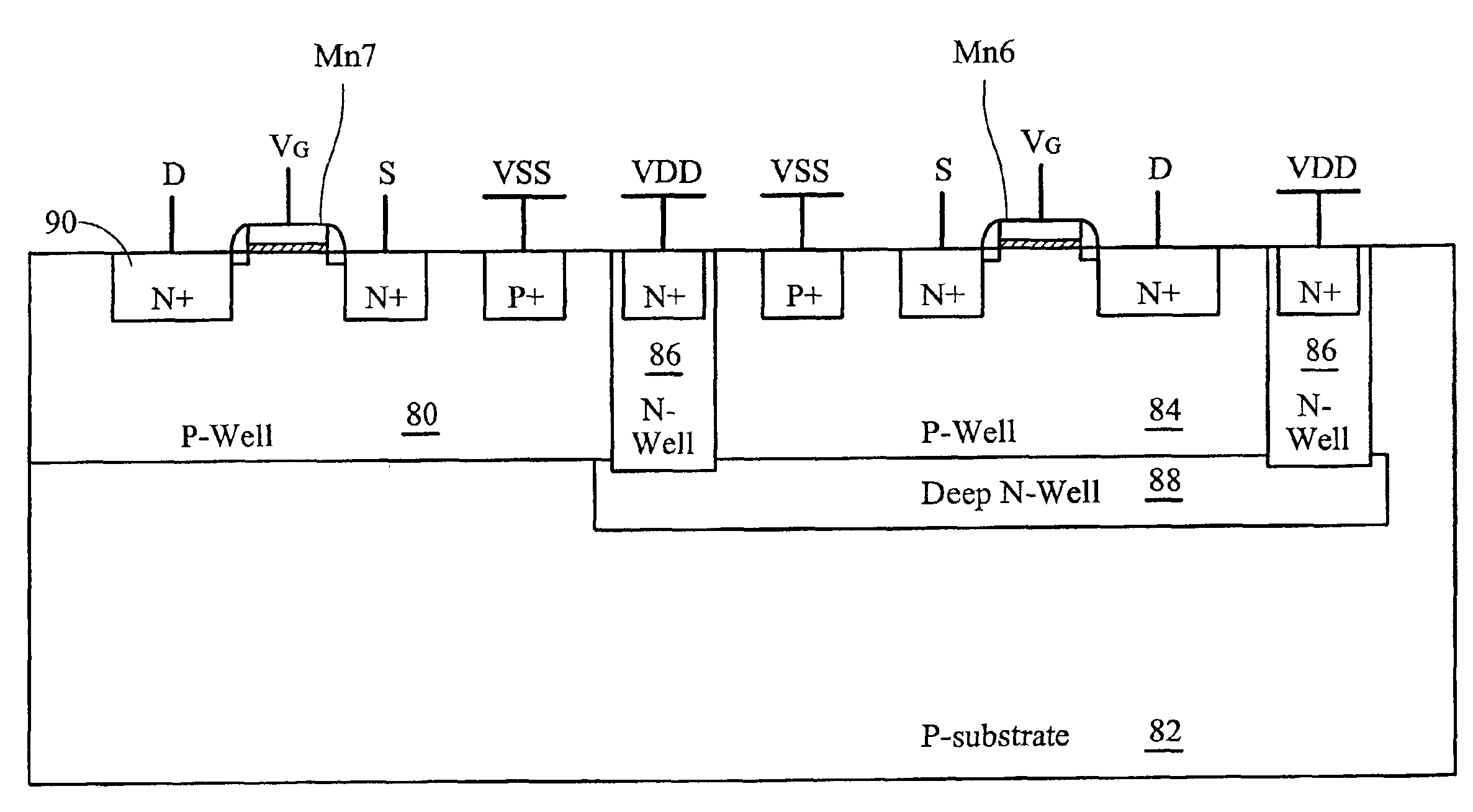
[0039]With the additional deep N-well structure as described in the prior art, an ESD protection design for overcoming the CDM ESD events is proposed in this invention. An ESD protection design using a deep N-well for overcoming CDM ESD events is proposed in the present invention. A cross-section of the NMOS component placed in an isolated p-well region with the deep N-well structure and the symbol thereof is shown in FIG. 7. The symbol shown in the right-hand side of the FIG. 7 will be used in the following section to show the ESD protection design against CDM ESD events. In FIG. 7, the stand-alone p-well 30 is isolated from the common substrate 34. The p-well 30 is coupled to VSS. The whole p-well region 30 is surrounded by a normal N-well 36 at the edge and a deep N-well 42 at the bottom. The N-well 36 the deep N-well 42 are biased at VDD via a N+ diffusion region 38. The stand-along p-well 30 is biased at a fixed voltage level, which, depending on the circuit design, is often a ...


PUM


Abstract

An object of the present invention is to provide a charged-device model (CDM) electrostatic discharge (ESD) protection circuit for an integrated circuit (IC). The ESD protection circuit comprises an ESD clamp device and a functional component. The ESD clamp device is coupled to a pad and a substrate having a first conductivity type. Under normal power operation, the ESD clamp device is closed. The functional component is formed on the substrate and coupled to the pad. The functional component has a first well having the first conductivity type and an isolating region having a second conductivity type for isolating the first well from the substrate. Under normal power operation, the functional component transmits signals between the IC and an external linkage. During an CDM ESD event, the CDM charges accumulated in the substrate are discharged via the ESD clamp circuit. Hence, the functional component is protected.

Description

BACKGROUND OF THE INVENTION[0001]1. Field of the Invention[0002]The present invention relates in general to a charged-device-model (CDM) electrostatic discharge (ESD) protection device, and especially to a CDM ESD protection device using deep N-well structure.[0003]2. Description of the Related Art[0004]ESD protection circuits are generally known to protect integrated circuits (IC) from machine model (MM) or human body model (HBM) electrostatic discharge events. In an HBM or MM mode electrostatic discharge event, electrostatic charges enter the IC through some of the IC pins and exit through others. To protect IC from such ESD events, an ESD protection circuit is often disposed adjacent to the output or input pad of the IC circuit to discharge the ESD stress. As the conventional ESD protection circuit shows in FIG. 1, the components of the input buffer 12 are protected against ESD events. The two-stage ESD protection circuit 10 has a secondary ESD protection circuit 14, a primary ES...

Claims


Application Information

Patent Timeline
IPC IPC(8): H01L23/58H01L23/60H02H9/00H02H3/20H02H3/22H01L27/02
CPCH01L27/0251
Inventor KER, MING-DOUCHANG, HUN-HSIENWANG, WEN-TAI
Owner TAIWAN SEMICON MFG CO LTD
Why Eureka
Try Eureka