
Relaxed silicon germanium substrate with low defect density

Inactive Publication Date: 2005-04-12
TAIWAN SEMICON MFG CO LTD
View PDF9 Cites 26 Cited by
  • Summary
  • Abstract
  • Description
  • Claims
  • Application Information

AI Technical Summary

Benefits of technology

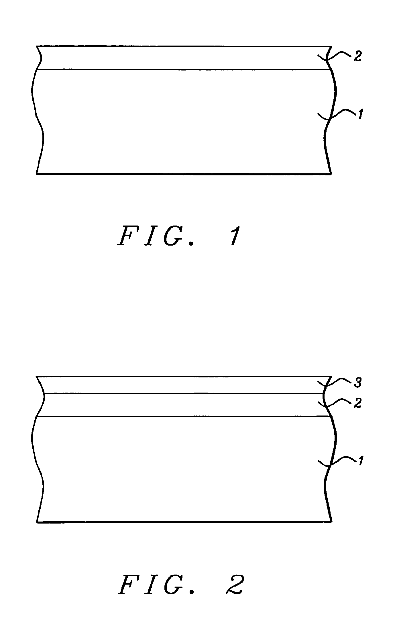
It is another object of this invention to form a composite layer comprised of a silicon layer, sandwiched between strained SiGe layers, and with increasing growth of the top SiGe layer create defects in the underlying silicon layer, while converting the overlying, strained SiGe layer to a relaxed, low defect density SiGe layer.

Problems solved by technology

However there are several disadvantages to the growth of a thick SiGe buffer layer.
First, a thick SiGe buffer layer at a thickness greater than a micrometer negatively impacts throughput adding unwanted processing costs.
The use of a thick SiGe buffer layer on a silicon on insulator (SOI) substrate, does allow defect densities to be decreased, however still in the unacceptable range of about 1E6 defects / cm2.

Method used


Image

  • Relaxed silicon germanium substrate with low defect density
  • Relaxed silicon germanium substrate with low defect density
  • Relaxed silicon germanium substrate with low defect density

Examples


first embodiment

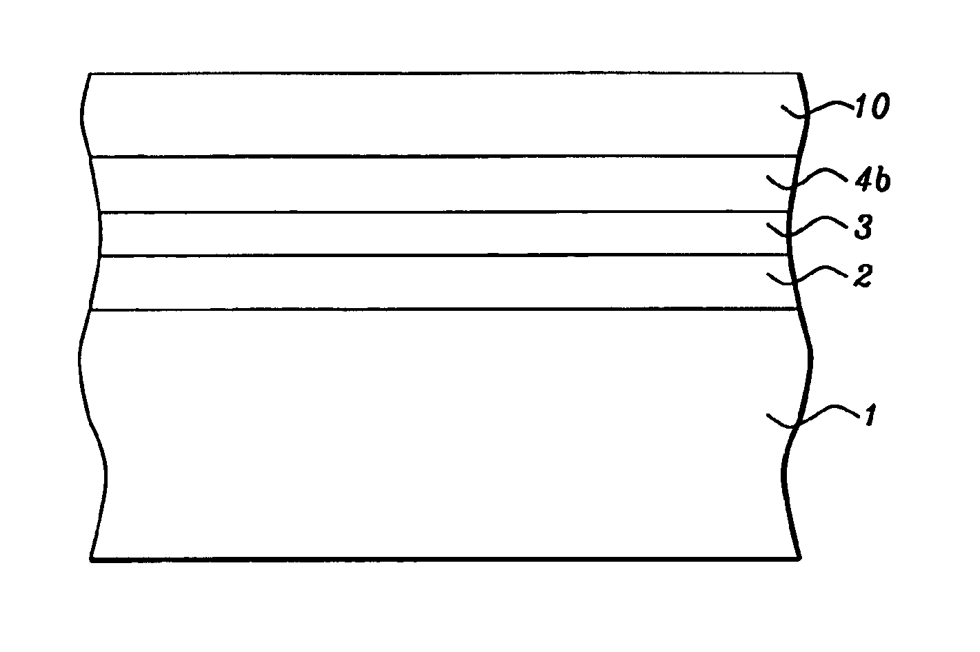
Critical, silicon layer 10, the desired layer to be used to accommodate the channel region for subsequent CMOS devices, is next epitaxially grown, and schematically shown in FIG. 5. Silicon layer 10, is epitaxially grown using silane or disilane as a source. The thickness of silicon layer 10, is less than it's critical thickness to maintain the desired strain in silicon layer 10. Thus the desired configuration needed to accommodate high performance, low leakage MOSFET devices, a strained silicon layer, on an underlying, relaxed low defect density layer, has been achieved via use of the above first embodiment of the invention.

second embodiment

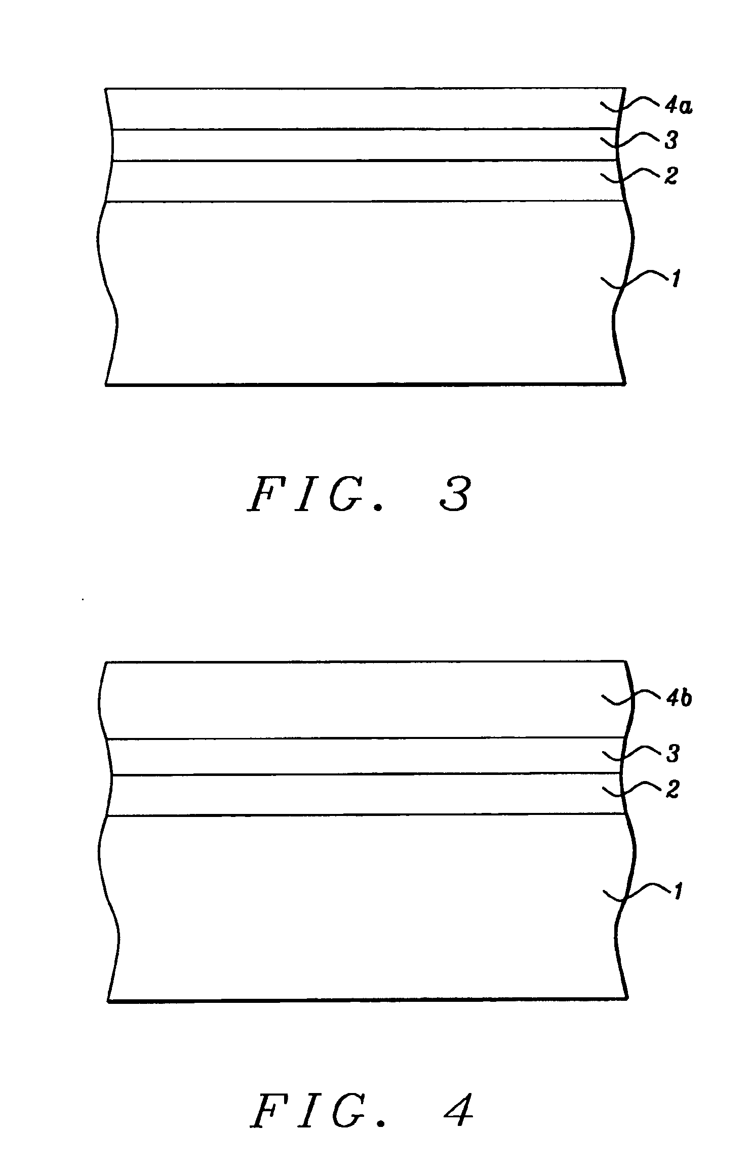
this invention, the process of forming a strained silicon layer on a relaxed, low defect density semiconductor layer, is next addressed and schematically shown using FIGS. 6-7. Epitaxial growth of the identical composite layer described in the previous embodiment via growth conditions, and using thicknesses identical to those used and previously described for the first embodiment of this invention, is again performed, however for this case followed by an anneal procedure. The anneal procedure results in additional relaxation of the overlying, SiGe layer, as well as additional decreases in defect density of this layer, when compared to counterpart SiGe layers not subjected to the anneal procedure. Anneal procedure 5, can be performed to thin, strained SiGe layer 4a, at a stage prior to completing the entire epitaxial growth procedure, then followed by additional epitaxial growth resulting in relaxed, low defect density, SiGe layer 4b, as shown schematically in FIG. 6. If desired the ...

third embodiment

this invention entails the use of ion implantation procedure 7, to weaken silicon layer 3, to allow overlying semiconductor alloy layer 4b, to be epitaxially grown again with increased relaxation and decreased defect density, when compared to counterpart layers formed on non-implanted, underlying silicon layers. The ability to obtain a relaxed, low defect density SiGe layer, improves the ability to subsequently grow a thin, strained silicon layer, under tensile strain. Growth of SiGe layer 4b, shown schematically in FIG. 8, featuring enhanced relaxation and low defect density, less than 1E3 defects / cm2, as a result of epitaxial growth on an underlying, implanted silicon layer, is next accomplished at an identical thickness, as well as using identical process parameters, as used with counterpart SiGe layers described in the previous embodiments. The attainment of SiGe layer 4b, featuring the improved parameters, again allows the epitaxial growth of strained silicon layer 10, to be ac...


PUM


Abstract

A method of forming a strained silicon layer on a relaxed, low defect density semiconductor alloy layer such as SiGe, has been developed. In a first embodiment of this invention the relaxed, low density SiGe layer is epitaxially grown on an silicon layer which in turn is located on an underlying SiGe layer. During the epitaxial growth of the overlying SiGe layer defects are formed in the underlying silicon layer resulting in the desired, relaxation, and decreased defect density for the SiGe layer. A second embodiment features an anneal procedure performed during growth of the relaxed SiGe layer, resulting in additional relaxation and decreased defect density, while a third embodiment features an anneal procedure performed to the underlying silicon layer prior to epitaxial growth of the relaxed SiGe layer, again allowing optimized relaxation and defect density to be realized for the SiGe layer. The ability to obtain a strained silicon layer on a relaxed, low defect density SiGe layer, allows devices with enhanced carrier mobility to be formed in the surface of the strained silicon layer, with decreased risk of leakage due the presence of the underlying, relaxed, low defect density SiGe layer.

Description

BACKGROUND OF THE INVENTION(1) Field of the InventionThe present invention relates to methods used to fabricate semiconductor devices, and more specifically to a method used to form a strained silicon layer to accommodate a channel region for a metal oxide semiconductor field effect transistor (MOSFET) device.(2) Description of Prior ArtA promising method for improving MOSFET device performance is enhancement of carrier mobility. Both hole and electron mobility enhancement can be accomplishment via the employment of surface channel, tensile strained silicon layers. Strained silicon layers used for MOSFET channel regions have been formed via epitaxial growth of silicon on relaxed silicon germanium (SiGe) pseudo substrates. Good film quality of strained silicon layers, and of relaxed SiGe layers, are important factors for enhanced performance of strained silicon MOSFET devices, however substrate layers exhibiting high defect density, in terms of dislocations, stacking faults, twins, e...

Claims


Application Information

Patent Timeline
IPC IPC(8): C30B1/00H01L21/36H01L21/00H01L21/20H01L21/70H01L21/02H01L21/84H01L21/205H01L21/324H01L29/10
CPCH01L21/02381H01L21/0245H01L29/1054H01L21/02532H01L21/324H01L21/02505
Inventor LIN, CHUN CHICHYEO, YEE-CHIAHUANG, CHIEN-CHAOWANG, CHAO-HSIUNGCHANG, TIEN-CHIHHU, CHENMINGYANG, FU-LIANGCHEN, SHIH-CHANGLIANG, MONG-SONGYAO, LIANG-GI
Owner TAIWAN SEMICON MFG CO LTD
Learn More