Method for forming pattern using printing process

a printing process and pattern technology, applied in the field of liquid crystal display devices, can solve the problems of reducing productivity, difficult to form an accurate alignment, and forming a fine pattern requiring a high degree of accuracy, and achieve the effect of accurate formation of fine patterns

Inactive Publication Date: 2005-04-05
LG DISPLAY CO LTD
View PDF24 Cites 11 Cited by
  • Summary
  • Abstract
  • Description
  • Claims
  • Application Information

AI Technical Summary

Benefits of technology

Another object of the present invention is to provide a method for forming a pattern, which is able to form a pattern on a liquid crystal display device with a single process in a printing method.
Another object of the present invention is to provide a method for forming a pattern, which is able to accurately form a fine pattern such as a passivation contact hole of a liquid crystal display device.

Problems solved by technology

Herein, it is difficult to form an accurate alignment due to a limitation of the exposing equipment.
Therefore, there is a limit in forming a fine pattern requiring a high degree of accuracy, and a plurality of photo processes should be repeated, thereby decreasing the productivity.

Method used


Image

  • Method for forming pattern using printing process
  • Method for forming pattern using printing process
  • Method for forming pattern using printing process

Examples


Embodiment Construction

Reference will now be made in detail to the preferred embodiments of the present invention, examples of which are illustrated in the accompanying drawings. Wherever possible, the same reference numbers will be used throughout the drawings to refer to the same or like parts.

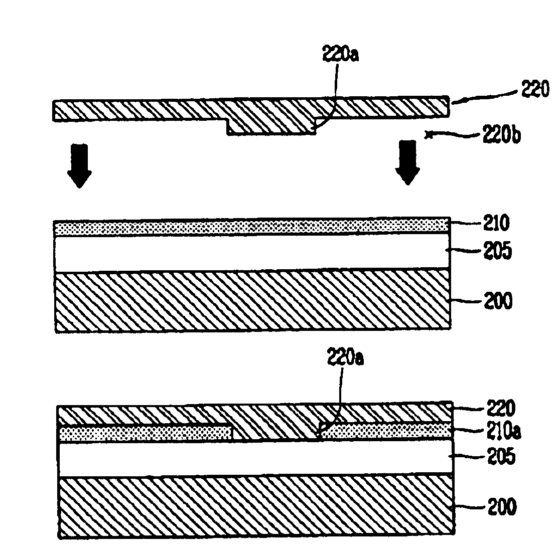
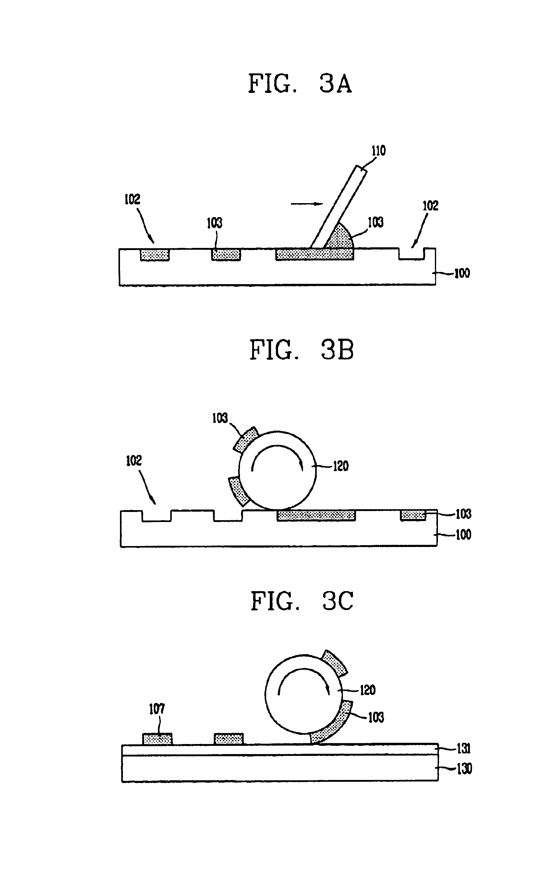
FIGS. 3A to 3C are cross-sectional views illustrating a resist pattern forming method in a liquid crystal display device through a printing method in accordance with the present invention.

With reference to FIG. 3A, a cliché100 with a concave groove 102 formed at a position corresponding to a pattern desired to be formed on a substrate is prepared. A resist 103 is deposited on the surface of the substrate 100. A doctor blade 110 may be used to planarize the surface of the cliché100, to push the resist into the grooves 102, and to remove the resist 103 from the surface of the cliché100. Thus, the resist 103 is filled in the groove 102 while the resist remaining on the surface of the cliché100 is removed.

As illustrat...


PUM

PropertyMeasurementUnit
widthaaaaaaaaaa
thicknessaaaaaaaaaa
insulatingaaaaaaaaaa

Abstract

A method for forming a pattern using a printing process is disclosed in the present invention. The method includes forming a resist layer on a substrate having an etching layer thereon, locating a master having a convex pattern over the substrate, pressing the master against the substrate until the convex pattern of the master directly contacts the etching layer, and removing a portion of the resist layer to expose a surface over the substrate, the removed portion of the resist layer having a width substantially the same as the convex portion of the master.

Description

This application claims the benefit of the Korean Patent Application No. P2002-081442 filed on Dec. 18, 2002, which is hereby incorporated by reference.BACKGROUND OF THE INVENTION1. Field of the InventionThe present invention relates to a liquid crystal display device, and more particularly, to a method for forming a pattern in a liquid crystal display device. Although the present invention is suitable for a wide scope of applications, it is particularly suitable for forming a fine pattern and increasing productivity.2. Discussion of the Related ArtIn display devices, particularly in flat panel display devices, pixels are arranged in a matrix form. Among the flat panel devices, liquid crystal display (LCD) devices have active devices, such as thin film transistors (hereinafter, TFTs), which are positioned in respective pixels for driving the pixels in the display devices. Such a method of driving the display device is called an active matrix driving method because the active devices...

Claims


Application Information

Patent Timeline
Patent Type & Authority Patents(United States)
IPC IPC(8): C03C25/68H01L21/302H01L21/02H01L21/461G02F1/1333G02F1/1362G03F7/00H05K3/00H05K3/06
CPCB82Y10/00B82Y40/00G02F1/1362G03F7/0002H05K3/0079H05K2203/1189H05K3/1275H05K2203/0113H05K2203/0143H05K2203/0534H05K3/061G02F1/1333
Inventor BAEK, MYOUNG-KEEPARK, KWON-SHIK
Owner LG DISPLAY CO LTD
Why Eureka
Try Eureka