Programmable resistance memory element with layered memory material
a memory element and layered technology, applied in the direction of bulk negative resistance effect devices, electrical equipment, semiconductor devices, etc., can solve the problem of limited use of these cells as a direct and universal replacement for present computer memory applications
- Summary
- Abstract
- Description
- Claims
- Application Information
AI Technical Summary
Benefits of technology
Problems solved by technology
Method used
Image
Examples
Embodiment Construction
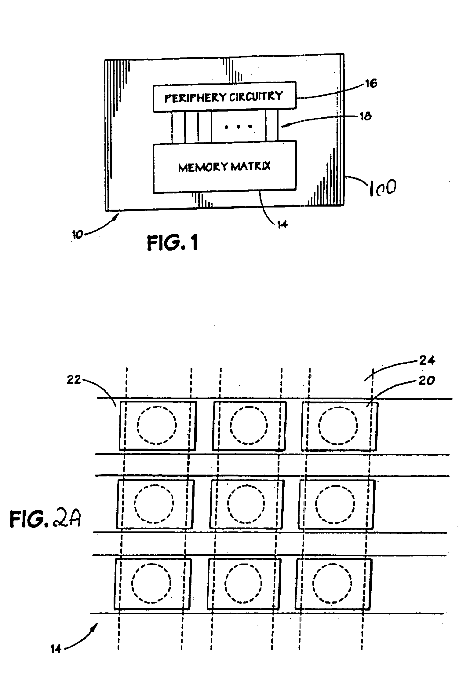
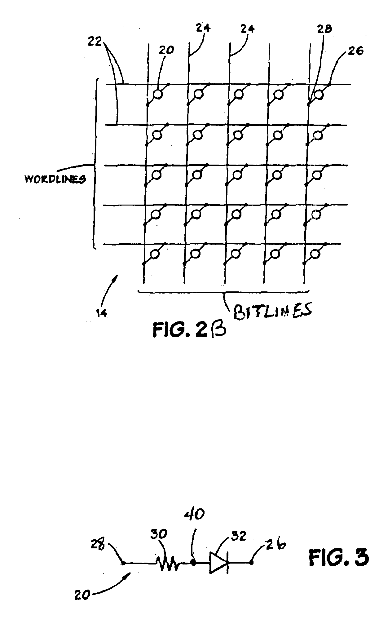
In the following paragraphs and association with the accompanying figures, examples of memory elements formed according to embodiments of the invention are presented. Specific embodiments of the memory elements and methods of making such memory elements are described as they might be implemented for use in semiconductor memory circuits. In the interest of clarity, not all features of an actual implementation are described in this specification.
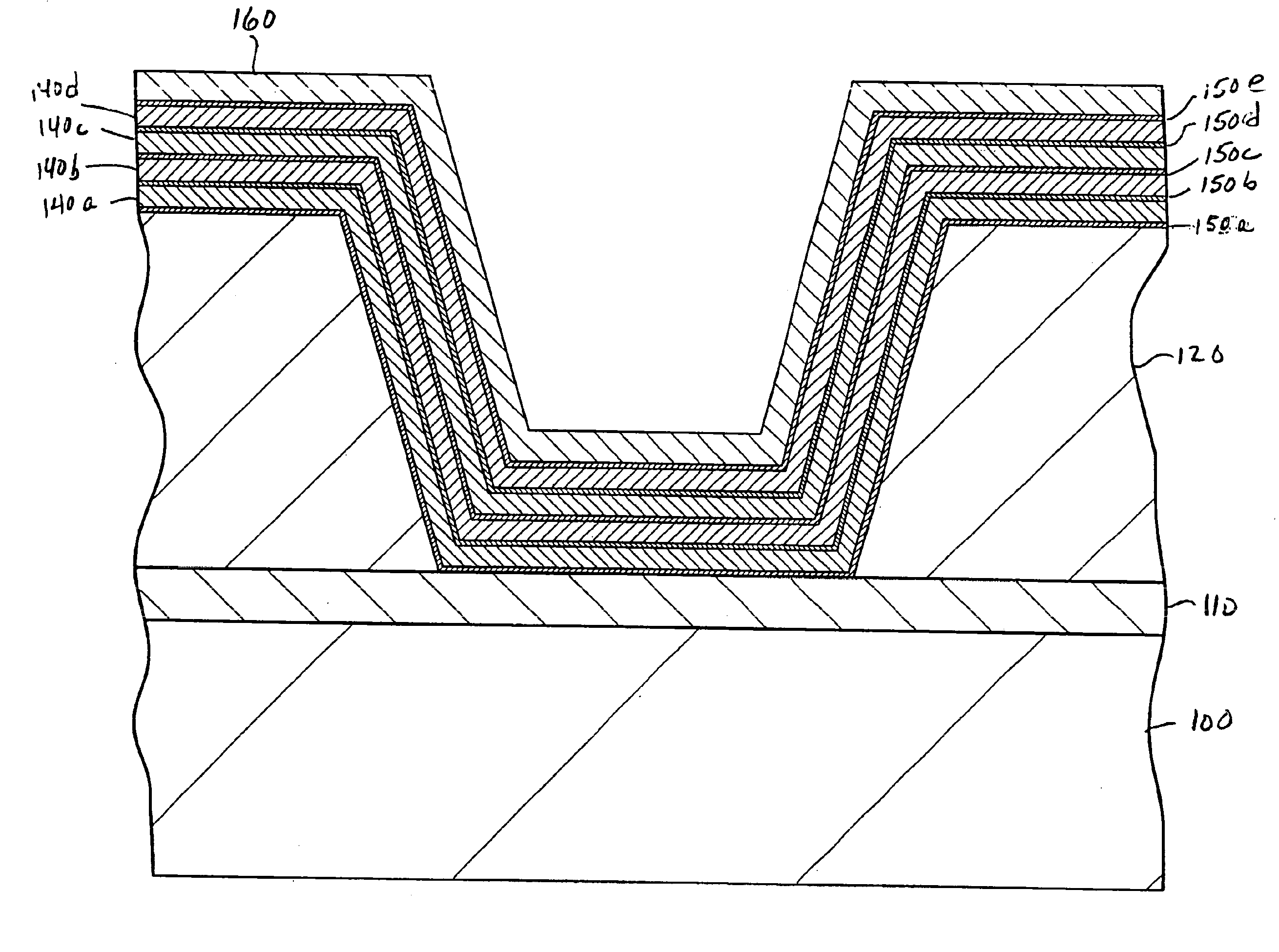
The present invention is directed to programmable resistance memory elements. The memory element includes a memory material. The memory material includes a programmable resistance material which is programmable between at least a first resistance state and a second resistance state in response to an electrical signal. The electrical signal is preferably an electrical current. The memory element further comprises one or more electrodes in electrical communication with the programmable resistance material. The one or more electrodes provide the ...
PUM
 Abstract
Description
Claims
Application Information
 - R&D
- Intellectual Property
- Life Sciences
- Materials
- Tech Scout
- Unparalleled Data Quality
- Higher Quality Content
- 60% Fewer Hallucinations
Browse by: Latest US Patents, China's latest patents, Technical Efficacy Thesaurus, Application Domain, Technology Topic, Popular Technical Reports.
© 2025 PatSnap. All rights reserved.Legal|Privacy policy|Modern Slavery Act Transparency Statement|Sitemap|About US| Contact US: help@patsnap.com


