
Methodology to characterize metal sheet resistance of copper damascene process

Inactive Publication Date: 2005-02-08
TAIWAN SEMICON MFG CO LTD
View PDF14 Cites 313 Cited by
  • Summary
  • Abstract
  • Description
  • Claims
  • Application Information

AI Technical Summary

Benefits of technology

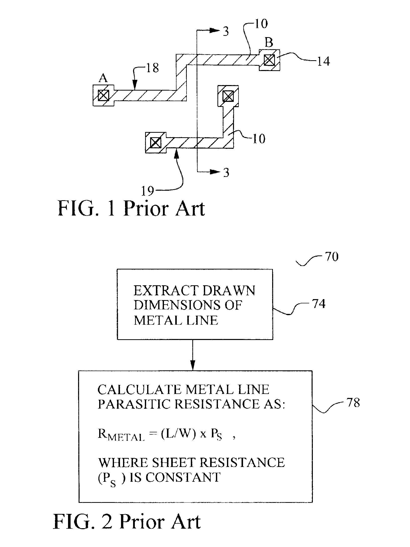
EDA tools may be used to model the performance of the circuit or of sub-sections of the circuit. For example, simulators, such as SPICE, have long been used to model analog performance or critical timing paths in circuits. A simulator will use standard models for active circuit elements, such as MOS transistors. A network of active devices is linked in a netlist file such that the combined performance of the circuit components may be simulated. The effect of parasitic RC values in the interconnects between active elements is typically included if it is available.

Problems solved by technology

As integrated circuit technology scales down, the impact of interconnect-induced delay becomes greater.
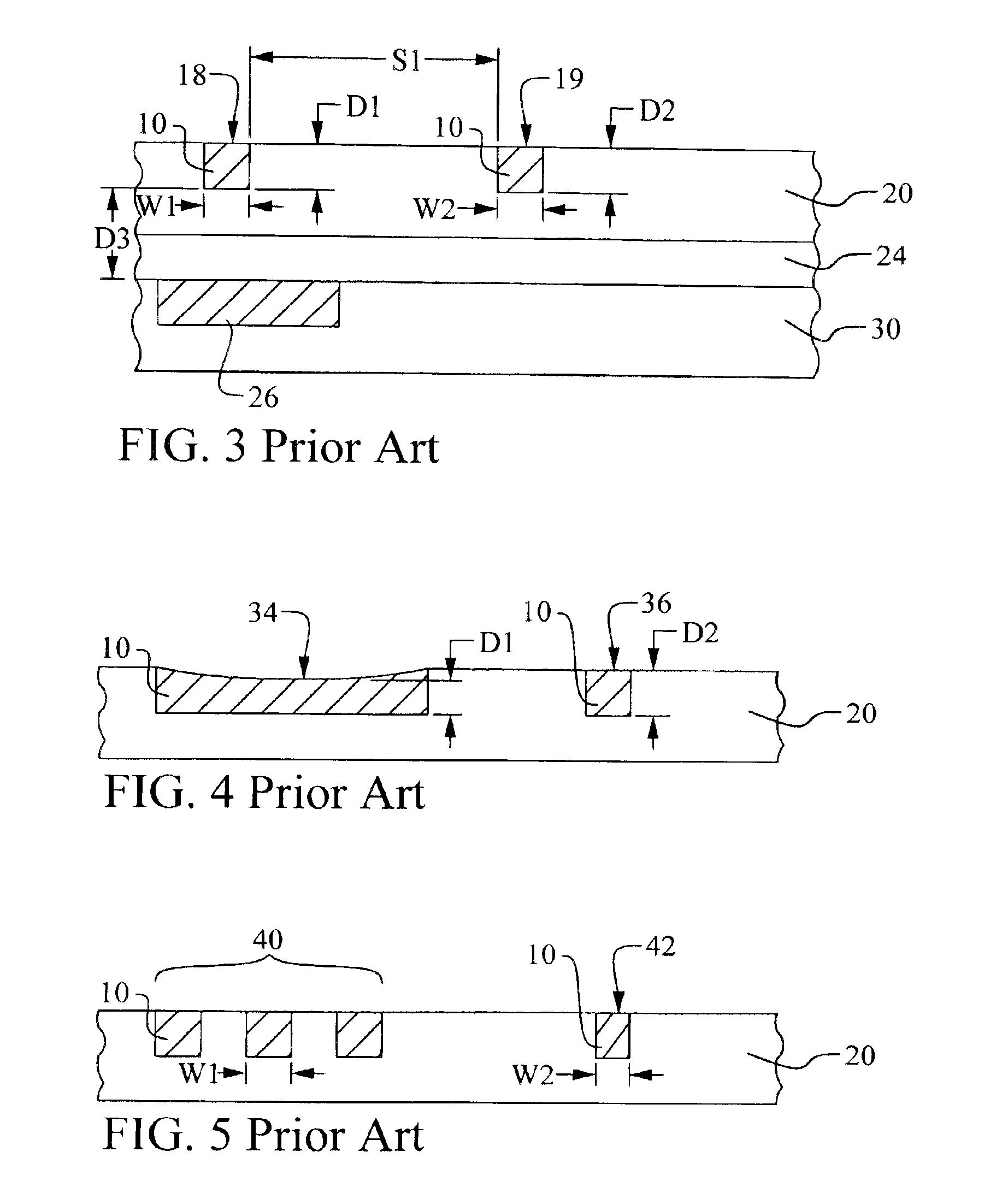
It is not typically possible to monitor interconnect thickness using a CD technique.
However, the assumption of uniformity may not be valid.
Adjacent features on the mask can create light interference that is transferred onto the photoresist pattern.
It is found that closely-spaced features will tend to be over-exposed.
This variation in physical widths W1 and W2 will cause the standard EDA parameter extraction to be in error.
If the EDA tool uses a constant value for the resistivity of the metal lines, then the results will be significantly in error.

Method used


Image

  • Methodology to characterize metal sheet resistance of copper damascene process
  • Methodology to characterize metal sheet resistance of copper damascene process
  • Methodology to characterize metal sheet resistance of copper damascene process

Examples


Embodiment Construction

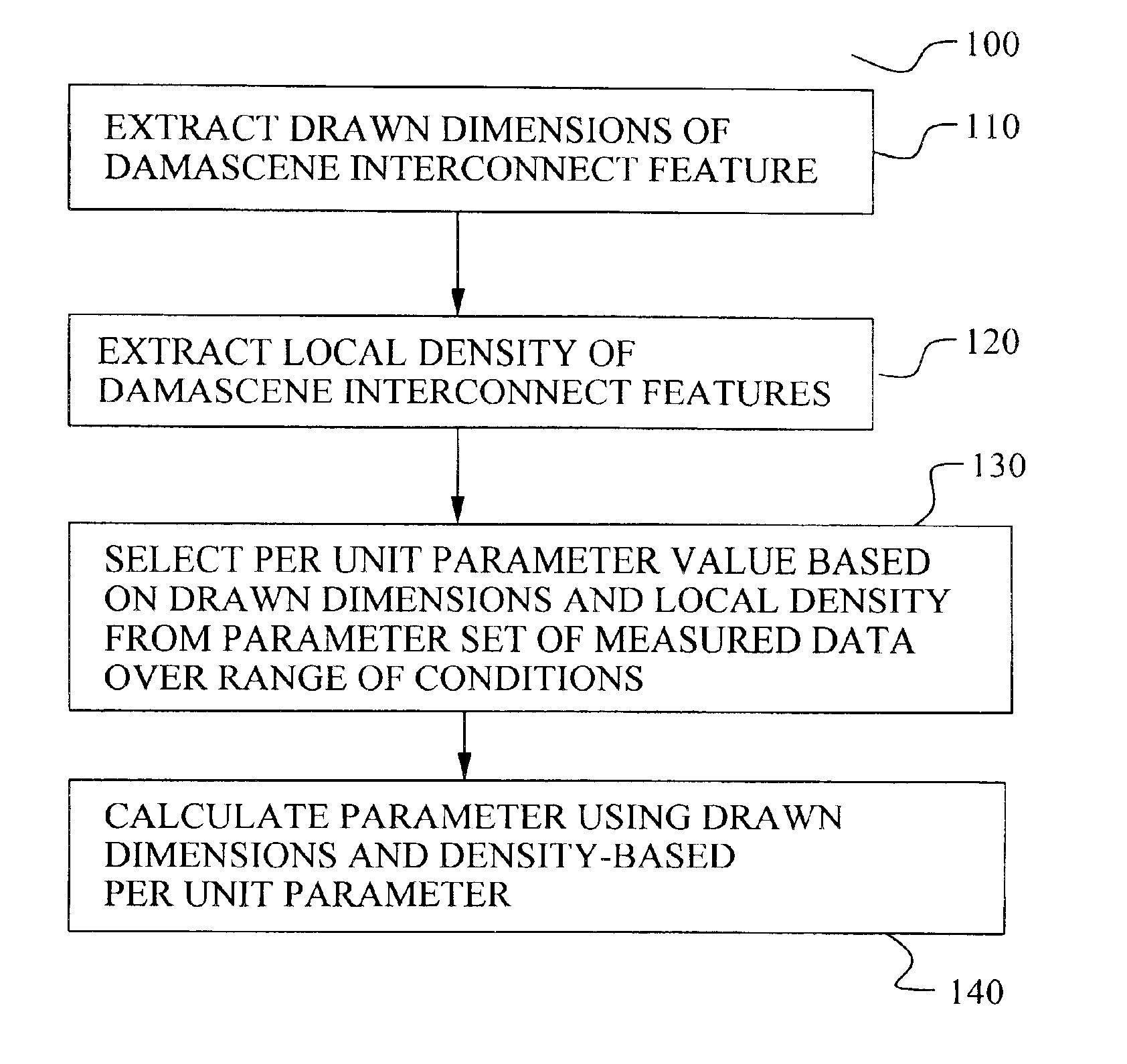
The preferred embodiments of the present invention disclose a method to determine a parameter of a damascene interconnect in an integrated circuit device is achieved. The method may be used to determine parasitic impedance of damascene metal lines based on characterization of the process over a range of drawn dimensions and local pattern densities. It should be clear to those experienced in the art that the present invention can be applied and extended without deviating from the scope of the present invention.

Referring now to FIG. 7, the preferred embodiment of the present invention is illustrated. Several important features of the present invention are shown and discussed below. The method 100 to determine a parameter of a damascene interconnect in an integrated circuit comprises several steps. The parameter can be, for example, resistance, parasitic capacitance, joule heating, current density or combinations thereof. First, drawn dimensions and local pattern density of a damascene...


PUM


Abstract

A new method to determine a parameter of a damascene interconnect in an integrated circuit device is achieved. Drawn dimensions and local pattern density of a damascene interconnect are extracted in an integrated circuit device. A parameter of the damascene interconnect is calculating using the drawn dimensions and the local pattern density to select a per unit value from a set of per unit values measured over a range of drawn dimension and pattern density combinations. The method may be used to improve the accuracy of extracted damascene metal line resistance and parasitic capacitance.

Description

BACKGROUND OF THE INVENTION(1) Field of the InventionThe invention relates to a method to determine a parameter of a damascene interconnect in an integrated circuit device and, more particularly, to a method to determine a parameter from a layout where the effects of dimension and local density, such as dishing, erosion, and optical proximity correction, are considered in the determination.(2) Description of the Prior ArtAs integrated circuit technology scales down, the impact of interconnect-induced delay becomes greater. That is, the parasitic resistance and capacitance (RC) of the interconnect system within the integrated circuit begins to play a greater role in the performance of the circuit. It is very important, therefore, that the parasitic RC components of the interconnect be modeled accurately.Referring now to FIG. 1, a simplified top view of a partial, integrated circuit is shown. In this layout, two metal interconnect lines 18 and 19 are shown. Each line is formed in a co...

Claims


Application Information

Patent Timeline
IPC IPC(8): G06F17/50H01L21/70H01L21/66H01L21/768H01L21/82
CPCG06F17/5036G06F30/367
Inventor CHUANG, HARRYCHANG, VICTOR C. Y.CHEN, YUNG-SHUNHOU, SHANG Y.
Owner TAIWAN SEMICON MFG CO LTD
Learn More