
Applying parametric test patterns for high pin count ASICs on low pin count testers

a parametric test pattern and parametric test technology, applied in the field of integrated circuit chip testers, can solve the problem of having to purchase expensive higher pin count testers

Inactive Publication Date: 2005-01-25
IBM CORP
View PDF19 Cites 86 Cited by
  • Summary
  • Abstract
  • Description
  • Claims
  • Application Information

AI Technical Summary

Benefits of technology

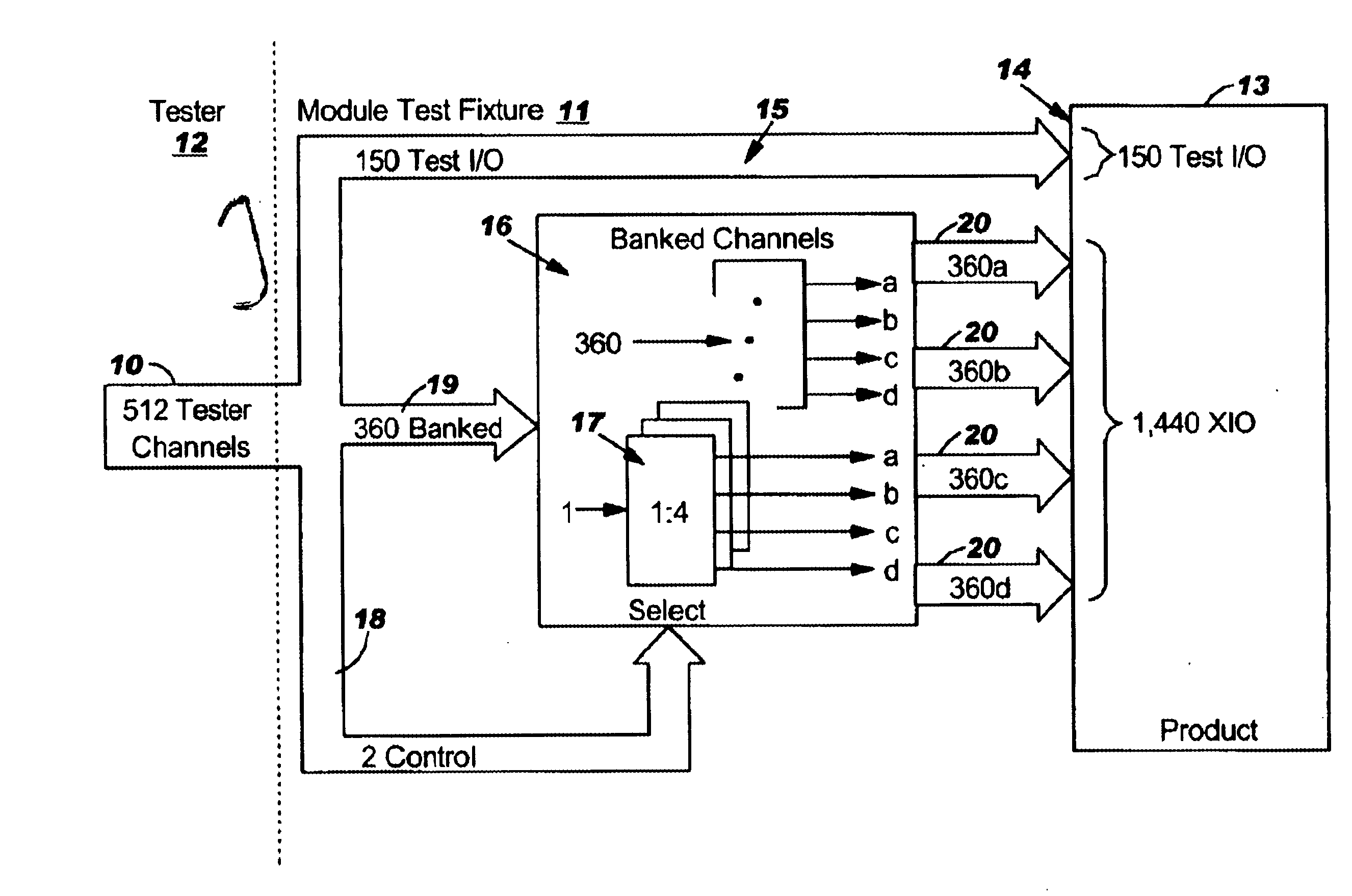
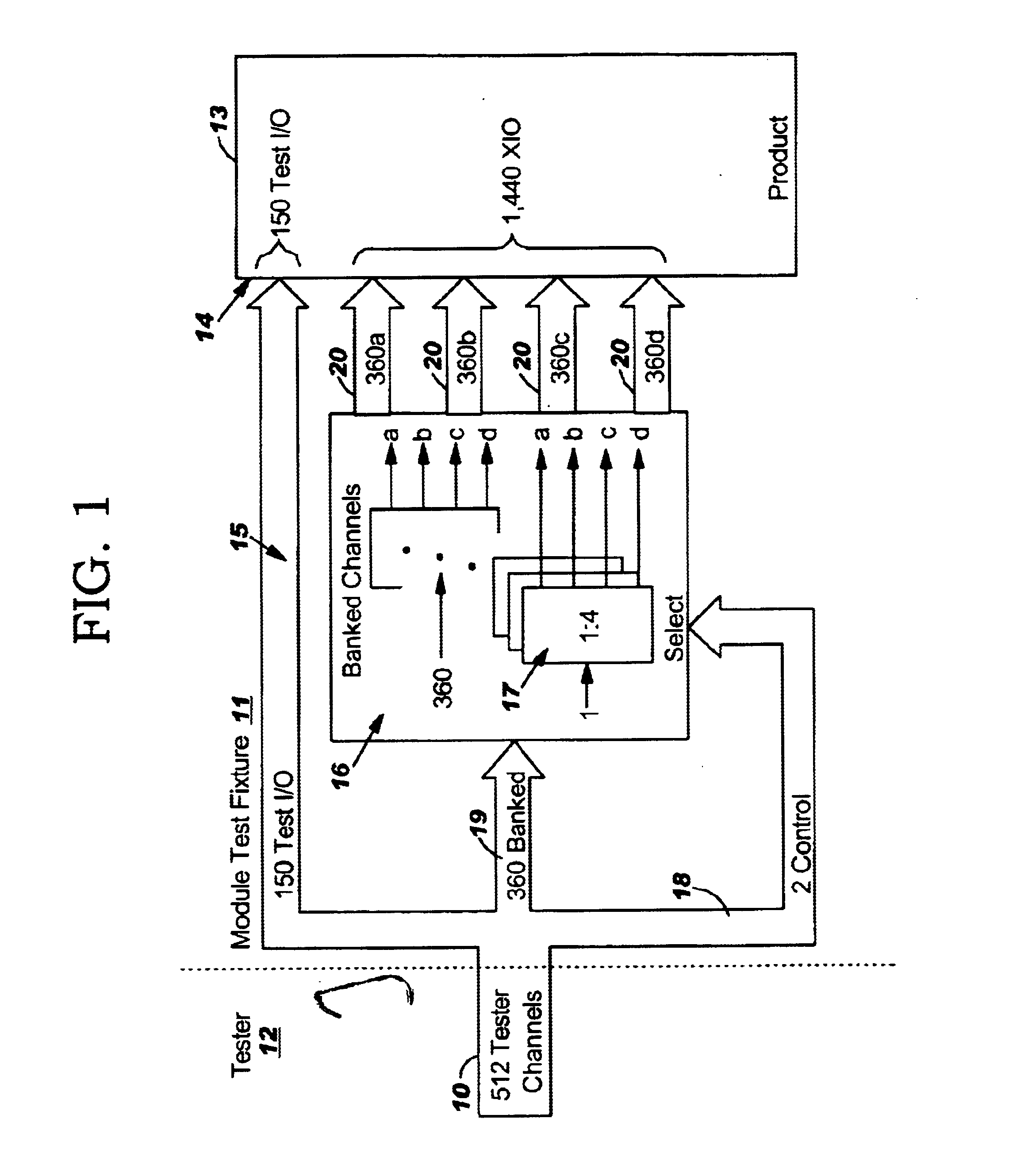
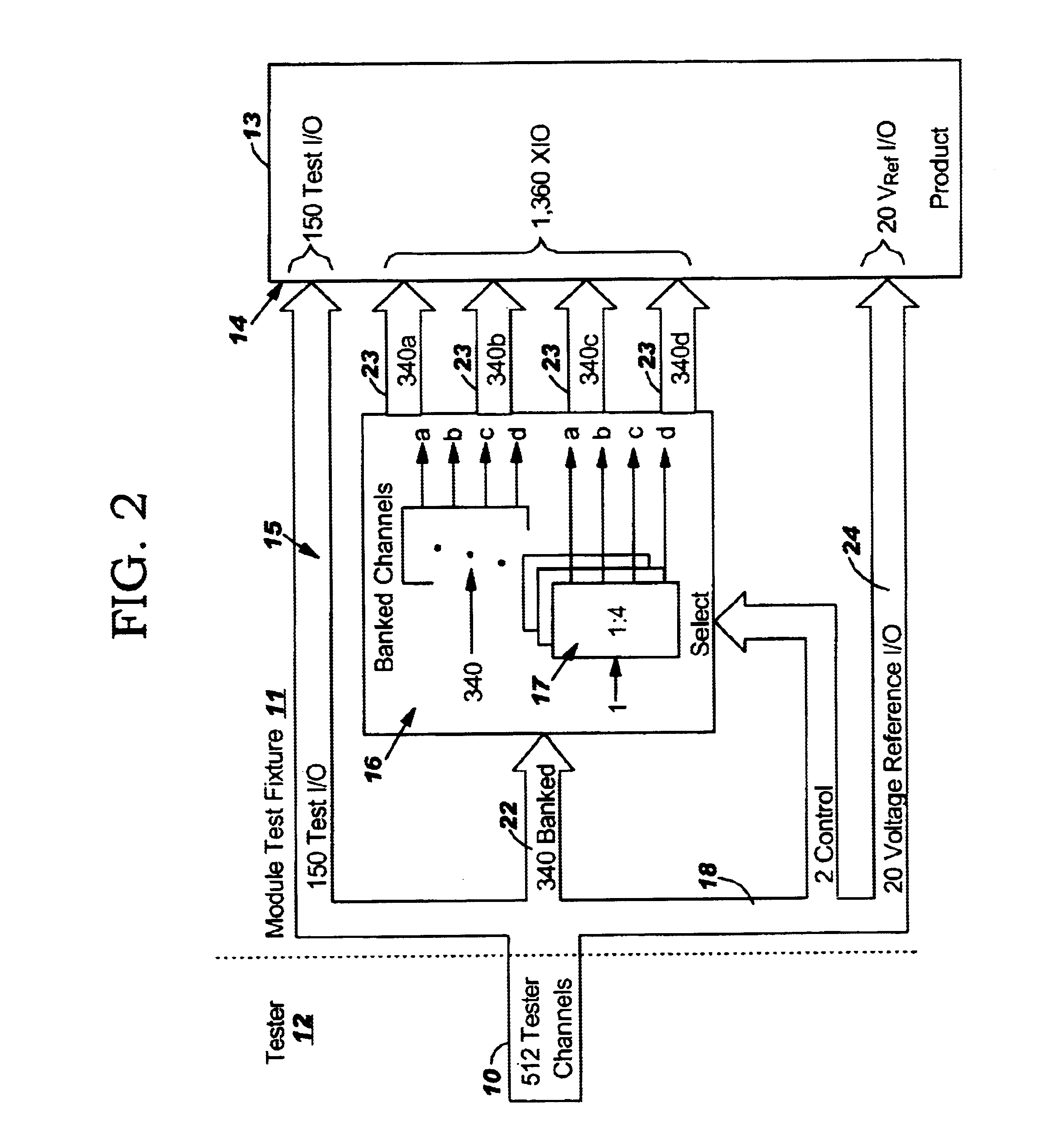
The present invention is an integrated circuit chip test apparatus that includes a module test fixture with contact pads for making contact with signal input / output pins on an integrated circuit chip being tested. An intermediate banking box is connected to the module text fixture and a tester is connected to the intermediate banking box. The tester includes at least one bank of channels for testing a portion of the integrated circuit that corresponds to the subset of pins. The selected channels are dedicated to specific pins and are not switched to different pins during chip testing. The intermediate banking box has a multiplexor controller for coordinating the connections of the banks. The invention allows for testing different types of chips with a single tester and intermediate banking box by modifying the full chip test program and connecting the intermediate banking box to different module text fixtures associated with different types of integrated chips.

Problems solved by technology

Presently, when products have pin counts and volumes that exceed the capacity of existing testers, expensive higher pin count testers must be purchased.

Method used


Image

  • Applying parametric test patterns for high pin count ASICs on low pin count testers
  • Applying parametric test patterns for high pin count ASICs on low pin count testers
  • Applying parametric test patterns for high pin count ASICs on low pin count testers

Examples


Embodiment Construction

This invention presents a Reduced Pin Count Test design and test methodology that allows parametric test patterns for high pin count ASICs to be applied using low pin count testers. The same boundary scan structure used to isolate the test of internal logic to a small number of test I / O is also used to apply parametric external I / O tests to the ASICs functional I / O. The parametric tests are banked into pin groups and applied on the same low pin count tester used for the internal logic tests. This results in substantial manufacturing test cost savings without loss of parametric fault coverage or test quality.

Using ASIC design and test methodologies, the parametric test patterns for high pin count products can be banked and applied by low pin count testers. The process used for “banking” is explained later in this paper. Complete parametric fault coverage is retained, thus allowing high quality test while avoiding the manufacturing cost of purchasing and operating high pin count teste...


PUM


Abstract

Disclosed is an integrated circuit chip test apparatus that has a module test fixture having contact pads that are adapted to make contact with signal input / output pins on an integrated circuit chip being tested. An intermediate banking box is connected to the module text fixture and a tester is connected to the intermediate banking box. The tester includes at least one bank of channels there are more pins on the integrated circuit chip than there are channels in the tester. The intermediate banking box includes switches that are connected between the contact pads and the channels. The switches are adapted to selectively connect a subset of the contact pads to the channels to connect the tester to a subset of pins, thereby allowing the tester to test a portion of the integrated circuit that corresponds to the subset of pins.

Description

BACKGROUND OF INVENTION1. Field of the InventionThe present invention generally relates to integrated circuit chip testers and more particularly to a universal banking box of switches that allow products to be tested on testers with fewer tester channels a product under test has pins.2. Background of InventionA product-design-specific Test Manufacturing Data (TMD) file is required for each ASIC logic product design. Since the TMD file is design-specific, creation of this file is typically the customers responsibility (some manufacturers offer Test Generation as a design service for ASIC customers). The TMD file contains a number of design-specific elements, including a complete gate-level logic model of the design and all the design-specific test patterns required to verify correct fabrication of the design.For some ASIC products, the TMD contains reduced pin count test (RPCT) patterns for the logic circuitry, cores, and embedded memory that are internal to a boundary scan chain. Th...

Claims


Application Information

Patent Timeline
Patent Type & Authority Patents(United States)
IPC IPC(8): G01R1/00G01R31/26G01R31/319
CPCG01R31/31926
Inventor CONTI, DENNIS R.LAFFERTY, JOHN
Owner IBM CORP
Learn More