
Power throughput adjustment in flash memory

Inactive Publication Date: 2005-01-18
ROUND ROCK RES LLC
View PDF5 Cites 47 Cited by
  • Summary
  • Abstract
  • Description
  • Claims
  • Application Information

AI Technical Summary

Benefits of technology

The embodiments of the present invention encompass a memory device that has a plurality of modes including a high data throughput mode and a low power mode. The device is comprised of a non-volatile memory location that stores a mode control bit. The state of the mode control bit selects one of the modes. In one embodiment, the mode control bit controls the rate at which data is programmed into the memory device's memory array, thereby controlling the power consumption.

Problems solved by technology

The designers typically have to trade off one for the other since the faster the programming, the higher the current consumption.
Similarly, the larger the number of bits programmed in parallel, the higher the current consumption.
This requires more time and money on the part of the designer.

Method used


Image

  • Power throughput adjustment in flash memory
  • Power throughput adjustment in flash memory
  • Power throughput adjustment in flash memory

Examples


Embodiment Construction

The embodiments of the present invention provide a memory device manufacturer with the ability to design one flash memory device that has a selectable low current consumption (i.e., low power) mode and a high data throughput mode. The mode is selectable by a latch that is programmed to select one of the modes. In one embodiment, this latch is permanently programmed with the desired mode at the time of manufacture.

While the subsequent discussion of the embodiments of the present invention refers to flash memory, any type of memory device that has similar characteristics may be used. For example non-volatile RAM (NOVRAM) or electrically erasable programmable read only memory (EEPROM) may be used.

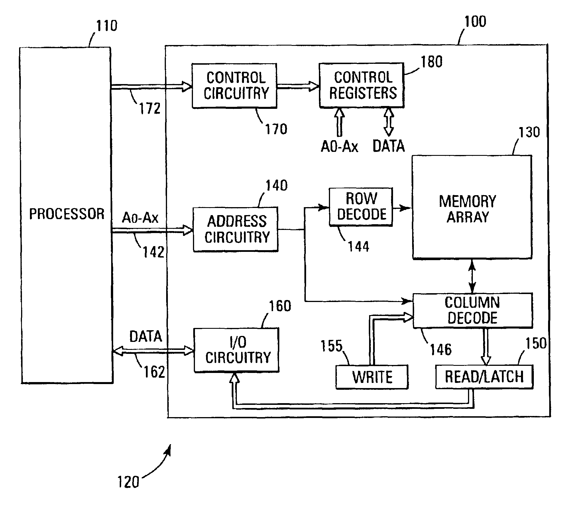
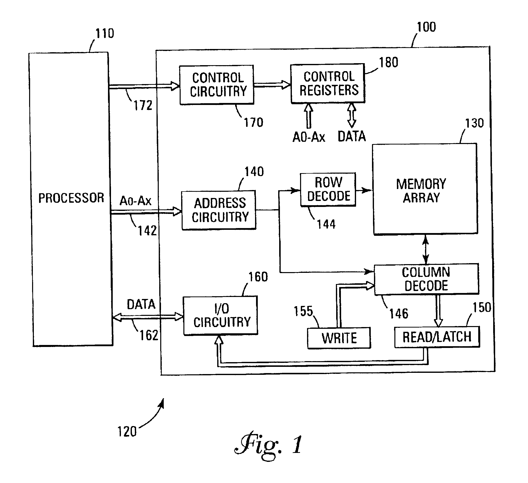
FIG. 1 is a functional block diagram of a memory device (100) of one embodiment of the present invention that is coupled to a processor (110). The memory device (100) and the processor (110) may form part of an electronic system (120). The processor (110) performs the operational tasks of the ...


PUM


Abstract

A mode control bit is used to adjust a mode of a memory device. The mode control bit is stored in a non-volatile memory location and selects between a data rate, low power consumption mode and a higher power, fast programming mode. In the low power consumption mode the mode control bit reduces the rate at which data bits are programmed into the memory device.

Description

BACKGROUND OF THE INVENTIONI. Field of the InventionThe present invention relates generally to programming flash memory and particularly to throughput adjustment.II. Description of the Related ArtFlash memory devices have developed into a popular source of non-volatile memory for a wide range of electronic applications. Flash memory devices typically use a one-transistor memory cell that allows for high memory densities, high reliability, and low power consumption. Common uses for flash memory include portable computers, personal digital assistants (PDAs), digital cameras, and cellular telephones. Program code, system data such as a basic input / output system (BIOS), and other firmware can typically be stored in flash memory devices.To encompass a large variety of applications, chip designers make some restrictive choices in the characteristics of the memory design. These characteristics include current consumption and programming speed or throughput. The designers typically have to ...

Claims


Application Information

Patent Timeline
IPC IPC(8): G11C16/30G11C16/06
CPCG11C29/028G11C16/30G11C16/04
Inventor CHEVALLIER, CHRISTOPHE J.
Owner ROUND ROCK RES LLC
Learn More