Semiconductor integrated circuit with stabilizing capacity

a technology of integrated circuit and stabilizer, which is applied in the direction of pulse generator, pulse technique, instruments, etc., can solve the problems of increasing the total amount of power consumed in the respective function blocks, reducing the stabilizing capacity of the voltage drop circuit. , to achieve the effect of reducing the parasitic capacity of output voltage, reducing the current consumption and reducing the stabilizing capacity of the voltage drop circui

Inactive Publication Date: 2005-01-04
RENESAS TECH CORP
View PDF6 Cites 16 Cited by
  • Summary
  • Abstract
  • Description
  • Claims
  • Application Information

AI Technical Summary

Benefits of technology

Therefore, according to the present invention, even in a case where the function blocks are brought into a standby state, it is possible to reduce a reduction in a parasitic capacity of output voltage (fist voltage) of the voltage drop circuit, so that there is produced an effect of reducing the stabilizing capacity of the voltage drop circuit built in the LSI without making the output of the voltage drop circuit unstable.
Moreover, according to the present invention, the voltage drop circuit has a driver supplied with the first voltage by the power supply voltage; a base voltage generating circuit that generates a base voltage; and a plurality of comparators each of which compares the base voltage with the first voltage, controls the driver so as to keep the first voltage at a predetermined value, has a different sensitivity, and is switched in response to variations in the first voltage. Therefore, there is produced an effect of reducing the current consumption of the voltage drop circuit in the standby state and optimizing the power consumption of the voltage drop circuit in the standby state and in the ordinary operating state.

Problems solved by technology

In a case of constituting an inexpensive system, however, there are many cases where a power supply voltage of a device other than an LSI can not be made lower and thus a voltage drop circuit is built in the LSI.
Moreover, while a need for the LSI used in a battery-driven type portable electronic device to decrease power consumption in a standby state has increased, the voltage drop circuit must have a comparator in itself and thus the power consumption of the voltage drop circuit itself becomes large, then the LSI in which the voltage drop circuit is built, presents a technical problem of reducing power consumption in the standby state.
The semiconductor integrated circuit in the prior art is constituted in the manner described above and thus presents the following problems.
Moreover, since the technology disclosed in the literature 2 has the voltage drop circuit for each function block, the technology not only has a disadvantage in area but also increases the total amount of power consumed in the respective function blocks.

Method used


Image

  • Semiconductor integrated circuit with stabilizing capacity
  • Semiconductor integrated circuit with stabilizing capacity
  • Semiconductor integrated circuit with stabilizing capacity

Examples


embodiment 1

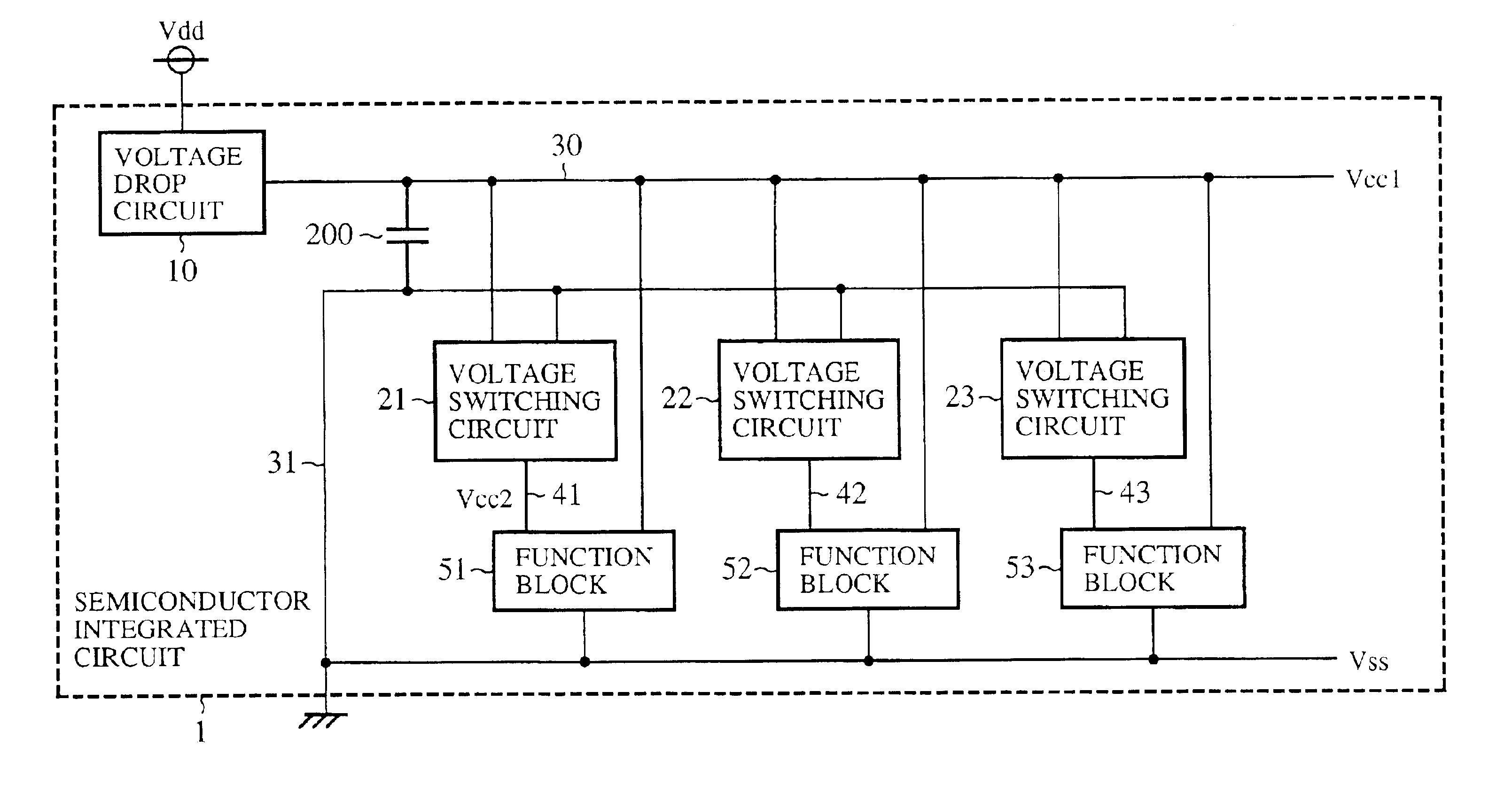
FIG. 1 is a block diagram to show a circuit constitution of a semiconductor integrated circuit with stabilizing capacity in accordance with embodiments 1 to 4 of the present invention. In the drawing, a reference symbol Vdd denotes a power supply voltage, Vss denotes a base voltage (for example, earth potential), 1 denotes a semiconductor integrated circuit, 10 denotes a voltage drop circuit that drops the power supply voltage Vdd to a voltage Vcc1 (first voltage) to output, each of 21, 22 and 23 denotes a voltage switching circuit that switches between the voltage Vcc1 and the base voltage Vss to produce a voltage Vcc2 (second voltage), 30 denotes a voltage line of output voltage Vcc1 of the voltage drop circuit 10, 31 denotes a voltage line of the base voltage Vss, each of 41, 42 and 43 denotes a voltage line of the output voltage Vcc2 outputted by each of the voltage switching circuits 21, 22 and 23. Each of 51, 52 and 53 denotes a function block supplied with the voltage Vcc1 an...

embodiment 2

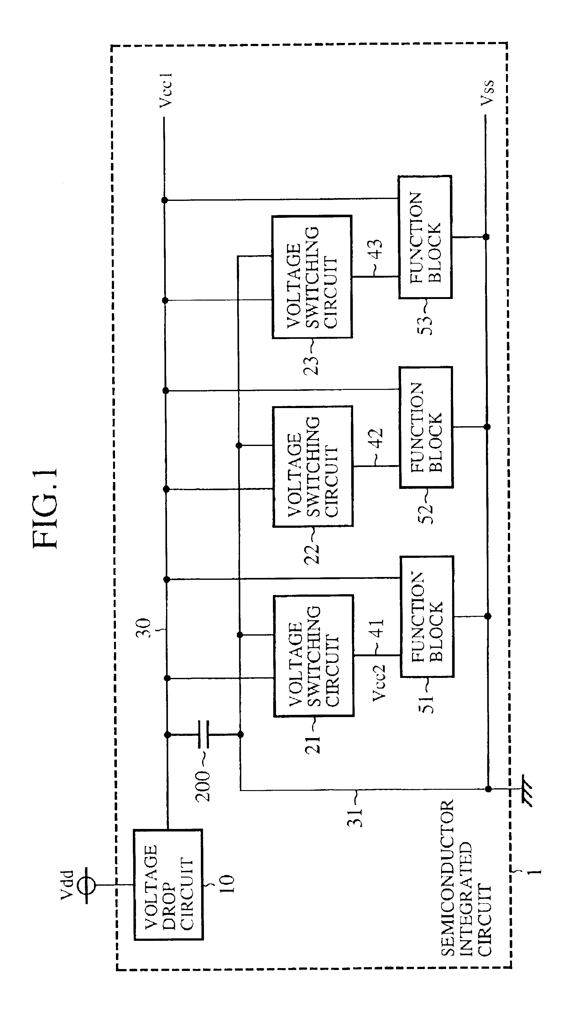
FIG. 5 is an explanatory diagram to show a schematic constitution of a logic gate in accordance with an embodiment 2 of the present invention. In the drawing, reference numerals 61, 62 denote gates of a Pch transistor and an Nch transistor that are not used for constituting a logic. The gates 61, 62 are connected to the line 30 of output voltage Vcc1 of the voltage drop circuit 10 and the source and the drain are connected to the voltage line 31 of the base voltage Vss.

In a case where the voltage Vcc2 is at the same potential as the voltage Vcc1, a fringe capacity of the gate 61 and an area capacity and a fringe capacity of the gate 62 function as capacities added to the stabilizing capacity 20 of the voltage drop circuit 10. In a case where the voltage Vcc2 is switched to the base voltage Vss, in addition to the capacity described above, an area capacity of the gate 61 functions as a capacity for stabilization, so that when the function blocks 51, 52 and 53 are brought into the sta...

embodiment 3

FIG. 6 is a circuit diagram to show a constitution of a voltage drop circuit in accordance with an embodiment 3 of the invention. In the drawing, reference numerals 102, 103 denote comparators and the comparator 102 is a type which has a higher sensitivity and a larger current consumption than those of the comparator 103. A reference numeral 105 denotes a driver that outputs voltage Vcc1, 111 denotes a reference voltage generating circuit that generates a predetermined reference voltage Vref1 of the voltage Vcc1.

Each of the comparators 102, 103 compares the reference voltage Vref1 generated by the reference voltage generating circuit 111 with the output voltage Vcc1 and, when the voltage Vcc1 becomes decreasing, controls the driver 105 so as to keep a predetermined value and the control is shared as follows by the comparators 102, 103.

In an ordinary operation in which all the function blocks 51, 52 and 53 are operated, because variations in the output voltage Vcc1 are large, the com...


PUM


Abstract

A semiconductor integrated circuit with stabilizing capacity has a voltage drop circuit that drops a power supply voltage to a first voltage Vcc1 and supplies the Vcc1 to a plurality of function blocks; a stabilizing capacity that stabilizes the Vcc1; and a plurality of voltage switching circuits each of which is provided in each of the function blocks and selectively switches between the Vcc1 and a base voltage Vss to produce a second voltage Vcc2 and supplies the Vcc2 to each function block, and each of the function blocks forms a capacity for stabilizing an output of the voltage drop circuit by means of its semiconductor structure by the Vcc1 and the Vcc2 applied thereto.

Description

BACKGROUND OF THE INVENTION1. Field of the InventionThe present invention relates to a semiconductor with a stabilizing capacity in which a plurality of integrated individual function blocks are arranged and in which a power supply unit capable of controlling an arbitrary individual function block in a standby state.2. Description of the Related ArtIn recent years, a semiconductor integrated circuit (hereinafter referred to as LSI) has been made in a finer process and thus in order to keep a dielectric strength and reliability of transistors, a power supply voltage to be applied is made lower. Moreover, there has been a trend to make a sub-threshold current passing through the transistors larger. In a case of constituting an inexpensive system, however, there are many cases where a power supply voltage of a device other than an LSI can not be made lower and thus a voltage drop circuit is built in the LSI. Because the voltage drop circuit needs a load capacity for stabilizing voltage...

Claims


Application Information

Patent Timeline
Patent Type & Authority Patents(United States)
IPC IPC(8): G05F1/10G05F1/46H01L27/04H01L21/822
CPCG05F1/465
Inventor OONISHI, KENJI
Owner RENESAS TECH CORP
Why Eureka
Try Eureka