
Wide operational range thermal sensor

a thermal sensor and wide-area technology, applied in the field of infrared radiation sensing, can solve the problems of low infrared sensitivity, low sensitivity of detector material, and low 1/f noise, and achieve the effects of low cost, low noise, and relatively simple silicon processing

Inactive Publication Date: 2005-01-04
NASA
View PDF25 Cites 5 Cited by
  • Summary
  • Abstract
  • Description
  • Claims
  • Application Information

AI Technical Summary

Benefits of technology

An important practical advantage in use of such (doped) silicon, as opposed to use of other semiconductors such as Ge and GaAs or of exotic materials such as VxOy is that silicon processing is relatively straightforward, inexpensive and does not require use of exotic processing regimes or exotic devices for electrical charge or voltage transfer. Silicon processing, with or without dopants present, has been fully developed and optimized over the last 50 years, and standard processing techniques and environments can be used to fabricate these thermal detectors. Silicon is relatively inexpensive to produce, compared with GaAs or VxOy. Formation of electrical contacts on a silicon detector is also straightforward and reliable, using contact materials such as ion implanted or diffused heavily doped silicon and epitaxial growth. The construction of arrays of Si bolometers can utilize well developed techniques for chemical etching and photolithography on a single wafer of Si. SiO2 and Si3N4 films are compatible with the Si processing steps used to mask bolometer sensors.

Problems solved by technology

Some high temperature superconductor bolometers, such as YBa2Cu3Ox deposited on a substrate of SrTiO3, operate within a very narrow range of temperatures, some as high as T=90 K, but over limited wavelength ranges and with high 1 / f noise that is not well understood.
Room temperature pyroelectric detectors, also discussed by Limperis and Mudar, op cit, may be operated at temperatures down to about 100 K, with the limitation that the detector responsivity for a given detector material falls dramatically with decreasing temperature.
Thermopile detectors, relying on a thermoelectric effect and discussed by Limperis and Mudar, op cit, have been used at moderate cryogenic temperatures for planetary and space exploration applications, with the limitation that they provide relatively low infrared sensitivity that does not increase adequately as temperature decreases.
A capacitive bolometer, which relies on temperature dependence of a dielectric constant or upon a loss coefficient of a ferroelectric glass ceramic, has not been developed for commercial use thus far, largely because of its low operating temperature requirements.
GaAs bolometers that operate at room temperature have been applied to sense submillimeter radiation by attachment to a carefully sized antenna but are very insensitive to changes in illumination.
GaAs is relatively costly and very difficult to purify for low temperature applications.

Method used


Image

  • Wide operational range thermal sensor
  • Wide operational range thermal sensor
  • Wide operational range thermal sensor

Examples


Embodiment Construction

Response of a bolometer to receipt of radiation is determined by the temperature coefficient of electrical resistance for the bolometer material

α=(1 / R)dR / dT.  (1)

For an impurity-doped semiconductor crystal, the temperature coefficient α is negative (conductivity increases with increasing temperature) and electrical resistivity is approximately

ρ={eN0μ(T)exp(EI / kBT)}−1,  (2)

where e is electronic charge, N0 is charge carrier concentration, μ(T) is mobility for the majority carrier, kB is the Boltzmann constant and EI is an impurity ionization energy. The ac electrical component of the bolometer response is proportional to

(ω)=−α√(R) / ω.  (3)

A larger value of is usually preferred.

A bolometer with resistance RB is often biased through a load resistance of about 10 RB, or higher. For practical electrical signal considerations, such as impedance load matching, RB=106 Ohms, and a 1 mm cube semiconductor crystal with resistivity ρ, the parameter can be computed for a suitable operating t...


PUM


Abstract

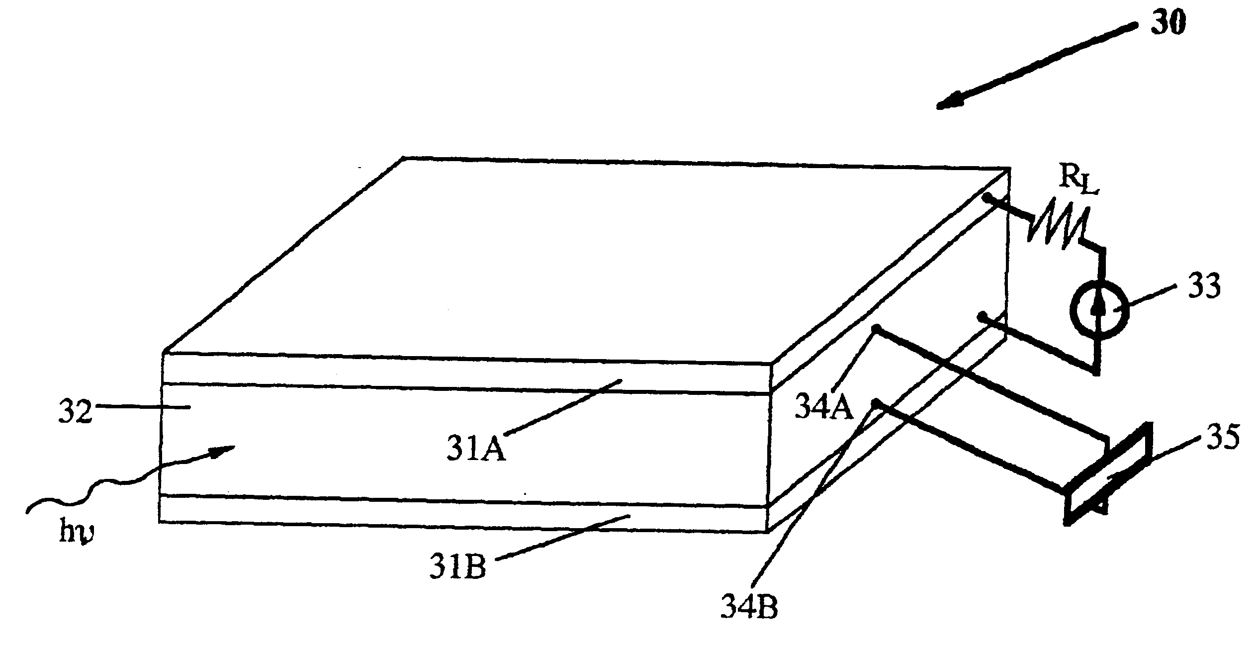
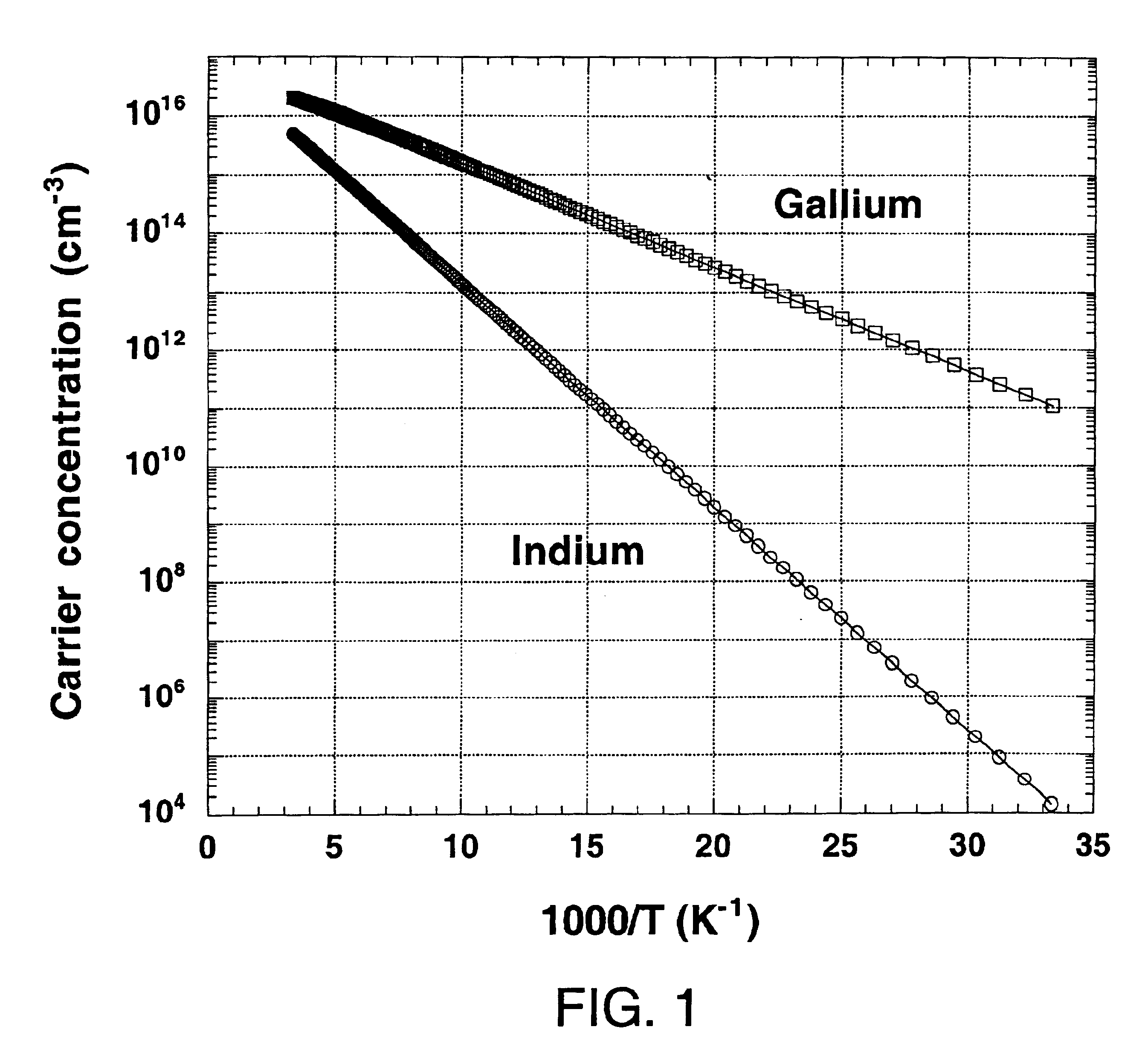
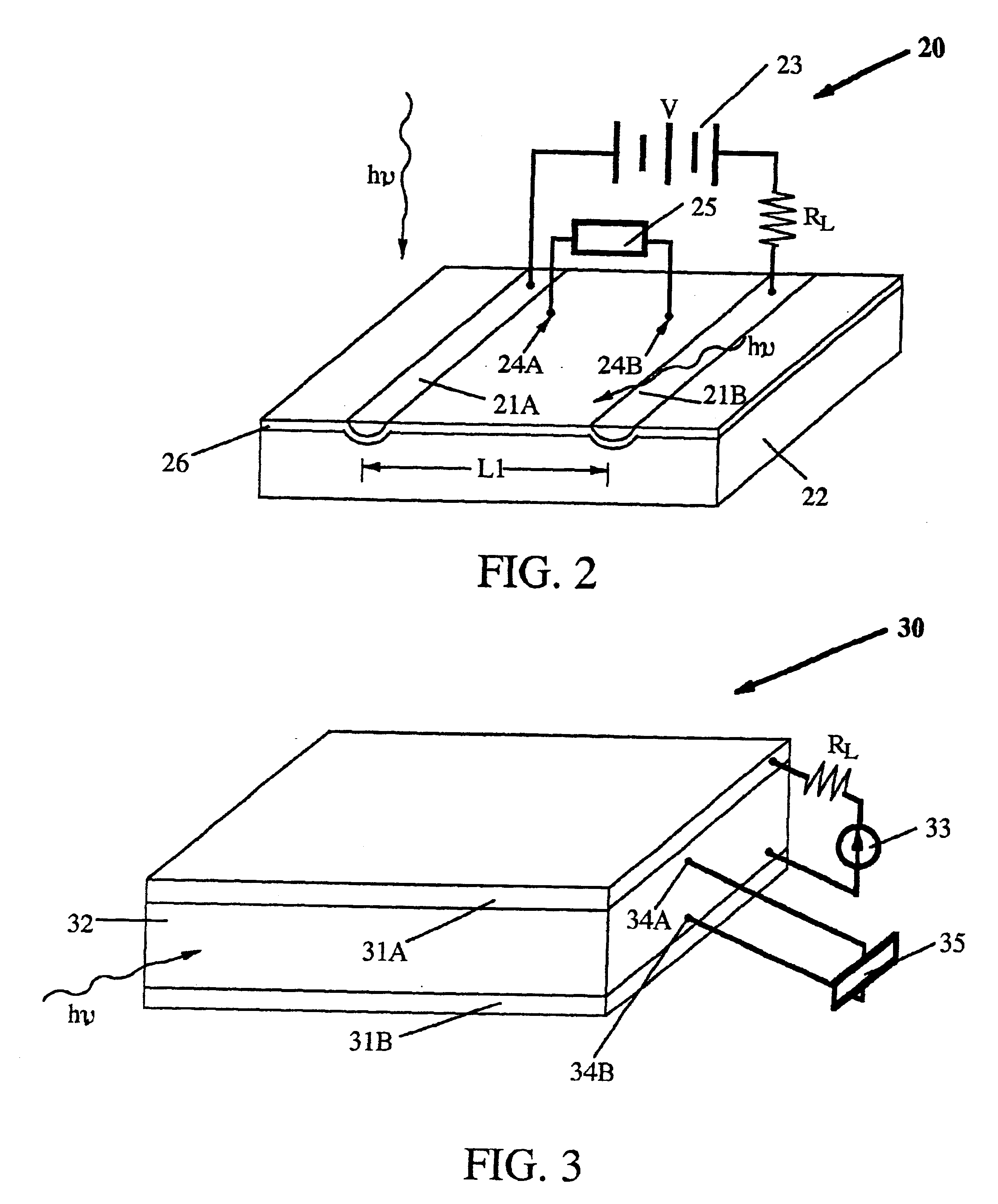
Bolometer system and method for detecting, at BLIP levels, presence of radiation over a broad range of wavelengths in an infrared spectrum and in a temperature range from 20 K to as high as room temperature. The radiation is received by a Si crystal having a region that is doped with one or more of In, Ga, S, Se, Te, B, Al, P, As and Sb in a concentration ratio in a range such as 5×10⁻¹¹ to 5×10⁻⁶. Change in electrical resistance ΔR due to receipt of the radiation is measured through a change in voltage difference or current within the crystal, and the quantity ΔR is converted to an estimate of the amount of radiation received. Optionally, incident radiation having an energy high enough to promote photoconductivity is removed before detection.

Description

ORIGIN OF THE INVENTIONThe invention disclosed herein was made by employees of the United States Government and may be manufactured and used by or for the Government for governmental purposes without payment of any royalties for such manufacture and use.1. Field of the InventionThis invention relates to sensing of infrared radiation using semiconductor materials.2. Background of the InventionIt is often desirable to detect the presence of infrared radiation across a large part of the infrared spectrum (e.g., 1-1000 μm) and at sensor temperatures from 30 K to 100 K, or even up to 300 K. One device, a resistive bolometer, detects such radiation by sensing a change in electrical resistance or conductivity of a thermally-sensitive component that reacts to presence of such radiation. Bolometers are discussed by T. Limperis and J. Mudar in “Detectors”, published in The Infrared Handbook, ed. by W. L. Wolfe and G. J. Zissis, Environmental Research Institute of Michigan, First Ed., Third Pr...

Claims


Application Information

Patent Timeline
IPC IPC(8): G01J5/20G01J5/24
CPCG01J5/24G01J5/20
Inventor GOEBEL, JOHN H.MCMURRAY, JR., ROBERT E.
Owner NASA
Learn More