Method for fabricating semiconductor device with loop line pattern structure

a semiconductor and pattern structure technology, applied in the direction of photomechanical treatment originals, instruments, optics, etc., can solve the problems of low throughput, high cost of manufacturing semiconductor products by using alt-psm, design complexity, etc., to simplify the overall process and eliminate the need for trim masks

Inactive Publication Date: 2004-11-16
PROMOS TECH INC
View PDF6 Cites 28 Cited by
  • Summary
  • Abstract
  • Description
  • Claims
  • Application Information

AI Technical Summary

Benefits of technology

In comparison with the alternating phase shift mask in the prior art, in which contact of each non-psm region and each alt-psm causes the need of a trim mask and double exposure process, the alternating phase shift mask according to the present invention has each non-psm region and each alt-psm region isolated from each other by an opaque loop, eliminates the need of the trim mask and simplifies the overall process.

Problems solved by technology

However, manufacturing semiconductor products by using an alt-psm is expensive and with low throughput.
However, such an optical lithography requires double exposure (because of the need of an alt-psm and a trim mask), leading to design complexity, difficulty in defect inspection and repair, and layout impact driven by the required trim at high resolutions.

Method used


Image

  • Method for fabricating semiconductor device with loop line pattern structure
  • Method for fabricating semiconductor device with loop line pattern structure
  • Method for fabricating semiconductor device with loop line pattern structure

Examples


Embodiment Construction

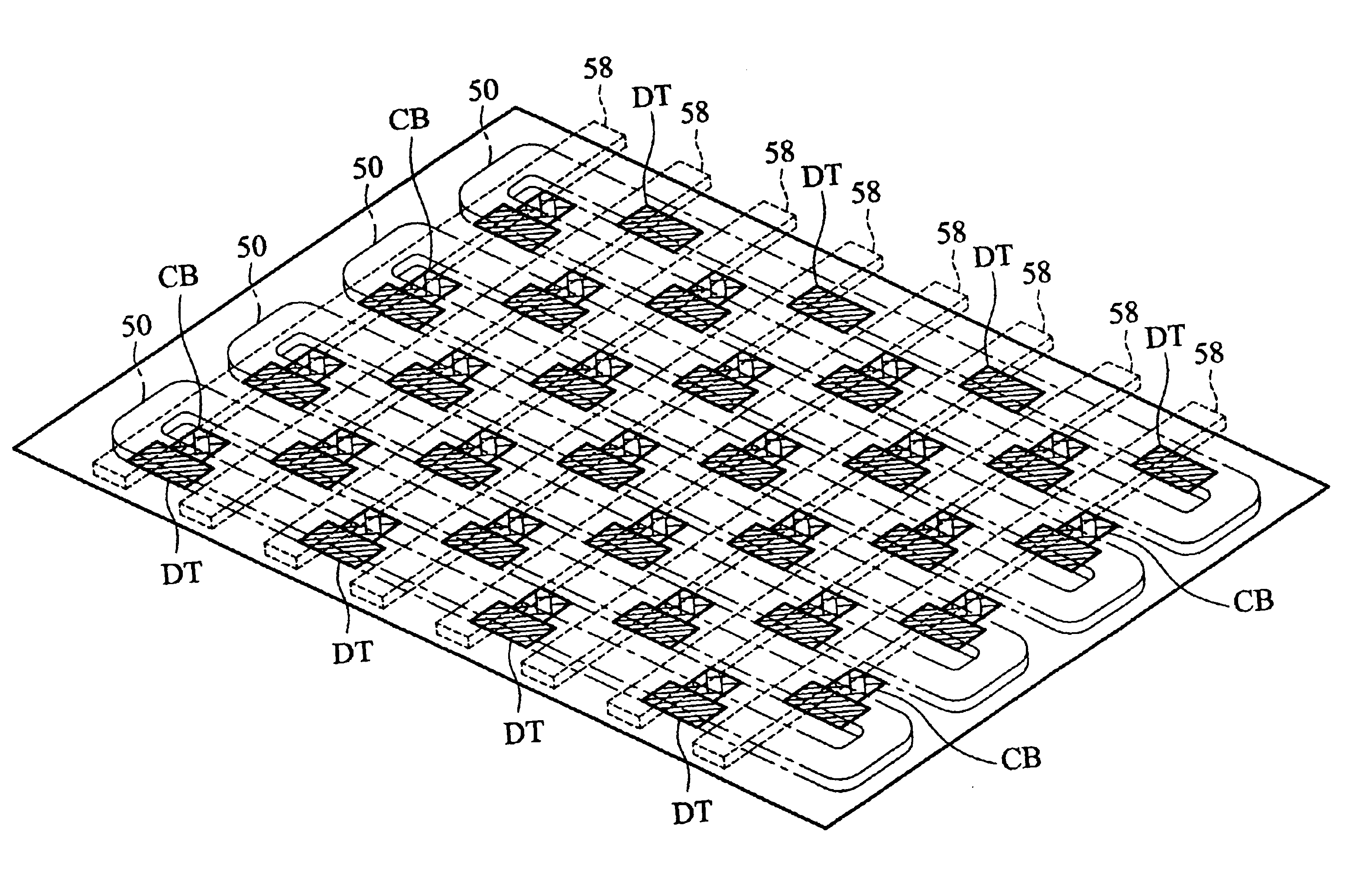
cell in FIG. 5B has a deep trench capacitor DT and shares a bit-line contact CB with an adjacent DRAM cell. FIG. 5B shows 4 gate-lines, each having a loop portion 50 corresponding to a dark loop 40 on the mask of FIG. 5A. Each loop portion So has a left straight portion 52 and a right straight portion 54. Taking the DRAM cell 56 for example, the left straight portion 52 passes above the deep trench capacitor of the DRAM cell 56 and has no effect for the cell's operation, while the right straight portion 54 passes the active area between the bit-line contact CB and the deep trench capacitor DT to consist a gate. Such a gate, as well-known in the art, controls the electric connection between the bit-line contact CB and the storage capacitor. Bit-lines will be formed by succeeding processes, each linking the DRAM cells at the same height. For example, the most bottom bit-line links the 4 DRAM cells at the bottom of the DRAM array in FIG. 5B. The cells having gates consisted of differen...


PUM

PropertyMeasurementUnit
feature sizeaaaaaaaaaa
phase differenceaaaaaaaaaa
transparentaaaaaaaaaa

Abstract

An alternating phase shift mask with dark loops thereon, a memory array fabricated with the alternating phase shift mask, and a method of fabricating the memory. The dark loops in the mask always separate first regions with 180° phase difference from second regions with 0° phase difference to define active areas or gate-lines in a DRAM chip.

Description

1. Field of the InventionThe present invention relates to a semiconductor device with loop pattern structure and a method of fabricating the same, which only needs an alternating phase shift mask (alt-psm) with single exposure process. The alternating phase shift mask used for fabricating the same is also disclosed.2. Description of the Related ArtRecently, phase shift technologies, instead of conventional chrome-on-glass (COG) technologies, have been incorporated into the design-to-silicon flow, allowing consistent and reliable reduction of IC feature size and providing a significant improvement in chip performance. As well, smaller feature size for ICs is less costly.FIG. 1 is a schematic diagram of a conventional COG technology. FIG. 2 is a schematic diagram of an alternating phase shift technology. As shown in FIG. 1, the COG technology uses binary mask, while the alternating phase-shift technology uses alternating phase shift mask (alt-psm), as shown in FIG. 2, having a neighbo...

Claims


Application Information

Patent Timeline
Patent Type & Authority Patents(United States)
IPC IPC(8): G03F9/00G03C5/00H01L21/70H01L21/02H01L21/336H01L27/108H01L21/8242G03F1/00H01L21/3213
CPCH01L21/32139H01L27/10861H01L27/10891G03F1/30H10B12/038H10B12/488
Inventor LEE, BRIAN S.LEE, CHIH-YU
Owner PROMOS TECH INC
Why Eureka
Try Eureka