Planarization method using fluid composition including chelating agents

Inactive Publication Date: 2001-08-28
MICRON TECH INC
View PDF17 Cites 5 Cited by
  • Summary
  • Abstract
  • Description
  • Claims
  • Application Information

AI Technical Summary

Benefits of technology

The planarization method of the present invention includes providing a wafer having a wafer surface. A pad is positioned for contact with the wafer surface and the wafer surface is planarized using the pad and a fluid composition including a chelating agent. The chelating agent may be one of any water so

Problems solved by technology

A large fraction of yield losses in wafer fabrication or processing of semiconductor devices is attributed to microcontamination.
Other damaging elemental impurities include heavy metals, for example, such as iron, copper, nickel, and gold.
The presence of contaminants during wafer processing has become particularly problematic in high density, large scale integration (LSI) technology.
For example, contaminants can cause a device to fail by improperly defining patterns, creating unpredictable surface topography, inducing leakage currents though insulating layers, or accelerating device wearout.
Generally, such fluid or slurries are quite pure; however, they are not free of contaminants such as the ionic contaminants listed above.
However, metal ions create contamination problems.
For example, such contaminants may diffuse into the surface of the wafer and down fracture paths.
However, such wet cleaning procedures are performed after CMP processing and contamination may have already caused significant contamination problems to the wafer during the CMP process.

Method used


Image

  • Planarization method using fluid composition including chelating agents
  • Planarization method using fluid composition including chelating agents
  • Planarization method using fluid composition including chelating agents

Examples


example 1

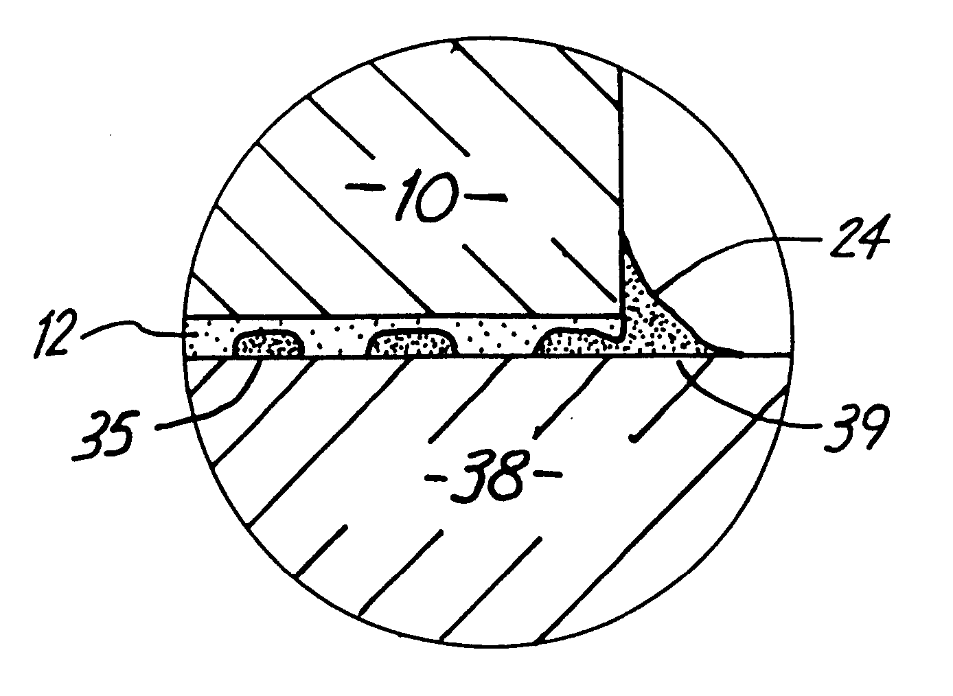
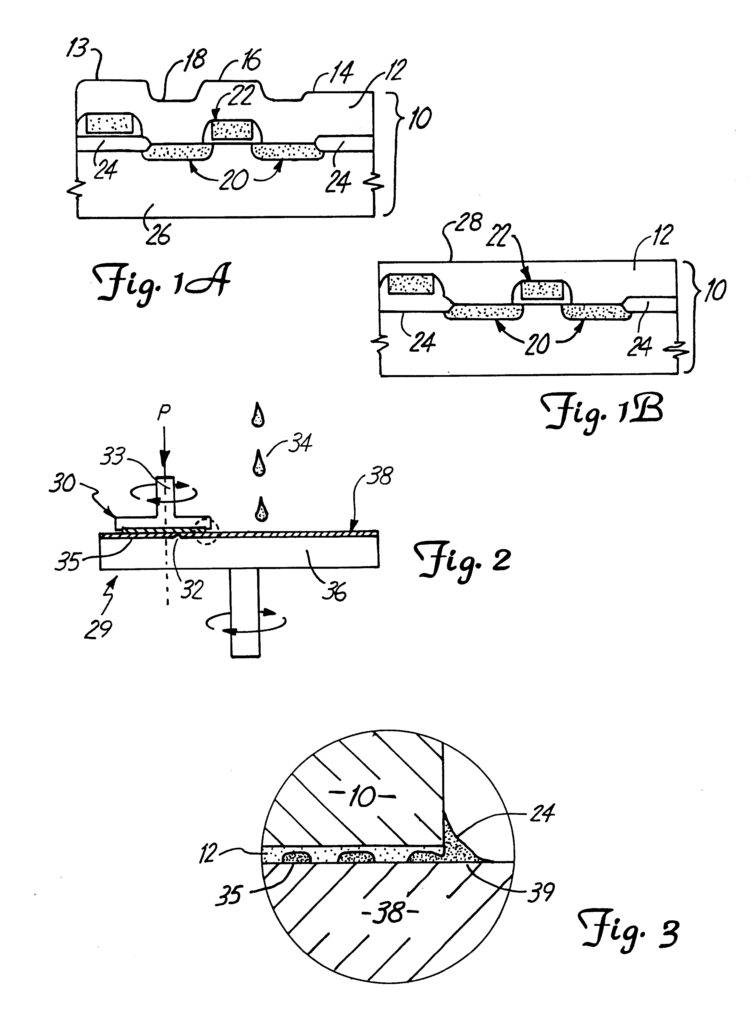
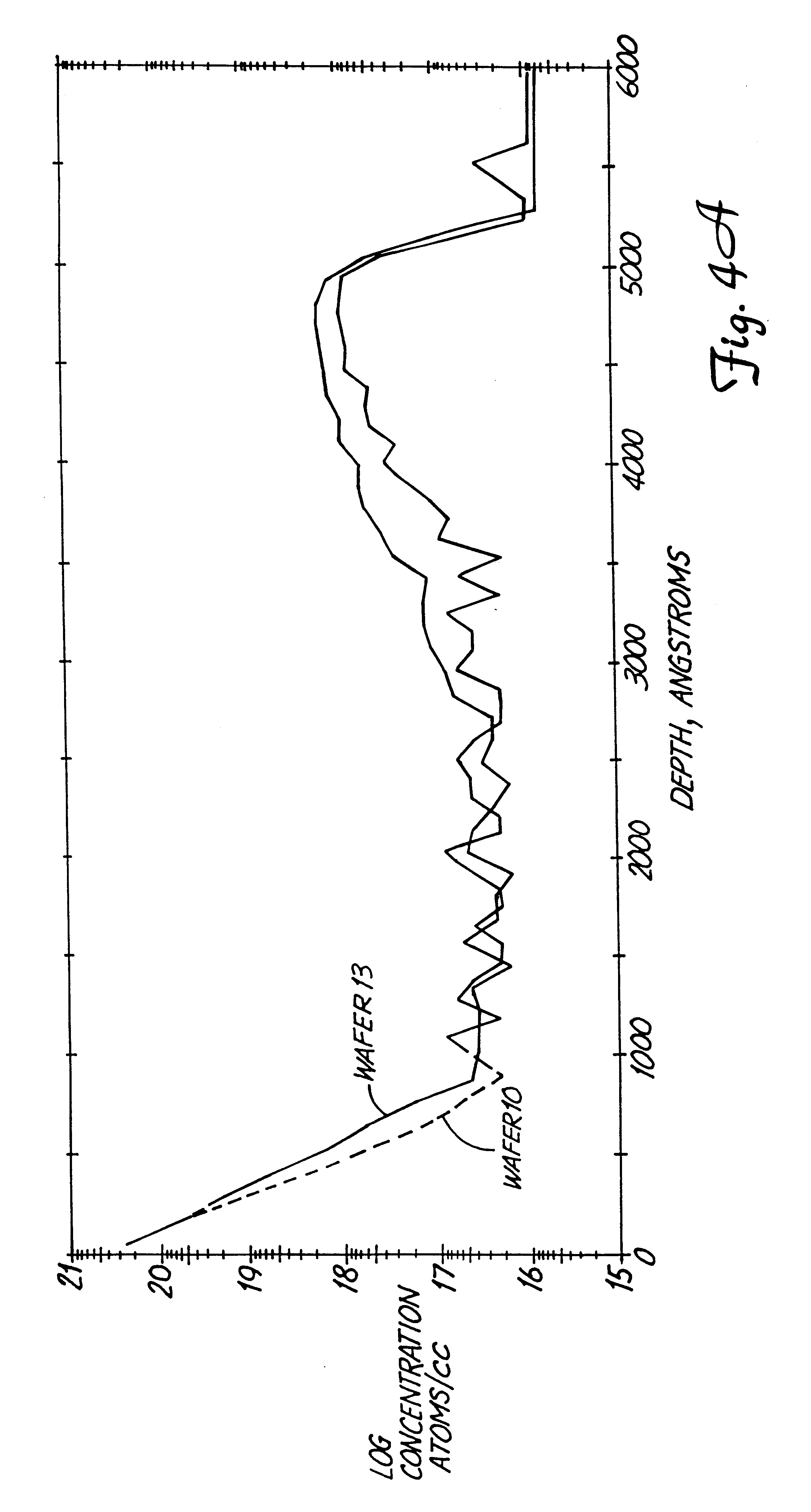
In this Example 1, four wafers were subjected to planarization. The CMP process was performed using a Westech CMP planarization unit, Model 372, available from IPEC / Westech. The four wafers were planarized for 1 minute and 53 seconds. The wafers undergoing planarization were all run with a 5 psi downforce pressure utilizing the wafer holder or carrier, a 2 psi backside pressure utilizing the wafer table or platen, carrier rotation at 28 rpm, platen rotation at 33 rpm, a 100 ml / mm flowrate of the slurry, and a wafer table or platen temperature of about 115.degree. F. All of the wafers were silicon wafers having BPSG deposited thereon; the BPSG layers being doped equally for each wafer and of a thickness of about 12,500 .ANG. BPSG. Between the planarization of each wafer, a pad conditioning step was performed which includes running a diamond studded disc across the pad, for a time period of about 75 seconds, to refresh the pad surface. After planarization, the two (BPSG / Si) wafers, 10...

example 2

In this Example 2, eight wafers were subjected to planarization. The CMP process was performed using a Westech CMP planarization unit, Model 472, available from IPEC / Westech. All the wafers were planarized for 20 seconds. When the conventional slurries were utilized with EDP, the slurry included 0.2 grams of EDP per 2 gallons of conventional slurry. The wafers undergoing planarization were all run with a 5 psi downforce pressure utilizing the wafer holder, a 2 psi backside pressure utilizing the wafer table, wafer table or platen rotation at 33 rpm, carrier or holder rotation at 28 rpm, a 100 ml / mm flowrate of the slurry, and a wafer table or platen temperature of about 115.degree. F. All of the wafers were silicon wafers having BPSG deposited thereon of about 3000 .ANG.. The BPSG layers were doped equally for each wafer. Between the planarization of each wafer, a pad conditioning step was performed which includes running a diamond studded disc across the pad, for a time period of a...

example 3

In this Example 3, three wafers were subjected to planarization. The CMP process was performed using a Westech CMP planarization unit, Model 472, available from Westech Systems, Inc. All wafers were planarized for 20 seconds. When the conventional slurries were utilized with EDP, the slurry included 0.2 grams of EDP per 2 gallons of conventional slurry. The wafers undergoing planarization were all run with a 5 psi downforce pressure utilizing the wafer holder, a 2 psi backside pressure utilizing the wafer table, table rotation of 33 rpm, carrier or holder rotation of 28 rpm, a 100 ml / mm flowrate of the slurry, and a wafer table or platen temperature of about 115.degree. F. All of the wafers were silicon wafers having BPSG deposited thereon of about 3000 .ANG.. The BPSG layers were doped equally for each wafer. Between the planarization of each wafer, a pad conditioning step was performed which includes running a diamond studded disc across the pad, for a time period of about 75 seco...


PUM

PropertyMeasurementUnit
Timeaaaaaaaaaa
Concentrationaaaaaaaaaa
Water solubilityaaaaaaaaaa

Abstract

A planarization method including the provision of a wafer having a wafer surface. A pad is positioned for contact with the wafer surface and the wafer surface is planarized using the pad and a fluid composition that includes a chelating agent. The chelating agent is a water soluble multidentate chelating agent, preferably a water soluble bidentate ionic chelating agent, and more preferably 1,2-ethylenediphosphonic acid (EDP). A fluid composition for use in planarization of a surface of a wafer includes a chemically interactive component that interacts with the surface of the wafer and a chelating agent for reducing the metal ion contamination of the wafer during planarization. The chelating agent may be one of a water soluble multidentate chelating agent, preferably a water soluble bidentate ionic chelating agent, and more preferably 1,2-ethylenediphosphonic acid (EDP). Further, the fluid composition may include an abrasive component.

Description

FIELD OF THE INVENTIONThe present invention pertains to planarization fluid compositions and planarization methods in the fabrication of semiconductor devices. More particularly, the present invention is directed to the use of chelating agents in such fluid compositions and methods.BACKGROUND OF THE INVENTIONA large fraction of yield losses in wafer fabrication or processing of semiconductor devices is attributed to microcontamination. Contaminants can be organic or inorganic particles, films or molecular compounds, ionic materials, or atomic species. Examples of ionic contaminants are sodium, potassium, lithium, calcium, boron, manganese, sodium, titanium, zirconium, aluminum, sulfur and magnesium. Other damaging elemental impurities include heavy metals, for example, such as iron, copper, nickel, and gold.The presence of contaminants during wafer processing has become particularly problematic in high density, large scale integration (LSI) technology. For example, contaminants can ...

Claims


Application Information

Patent Timeline
IPC IPC(8): C09G1/00C09G1/02H01L21/02H01L21/306H01L21/3105
CPCC09G1/02H01L21/31053H01L21/02024
Inventor SKROVAN, JOHNMEIKLE, SCOTT
Owner MICRON TECH INC
Why Eureka
Try Eureka