
Semiconductor device and method of fabricating the same

a technology of semiconductor devices and semiconductor materials, applied in semiconductor devices, semiconductor/solid-state device details, electrical apparatus, etc., can solve problems such as discontinuity at conductive parts, insufficient improvement, and difficulty in filling through-holes such as wiring materials

Inactive Publication Date: 2000-08-22
SEIKO EPSON CORP
View PDF10 Cites 32 Cited by
  • Summary
  • Abstract
  • Description
  • Claims
  • Application Information

AI Technical Summary

Benefits of technology

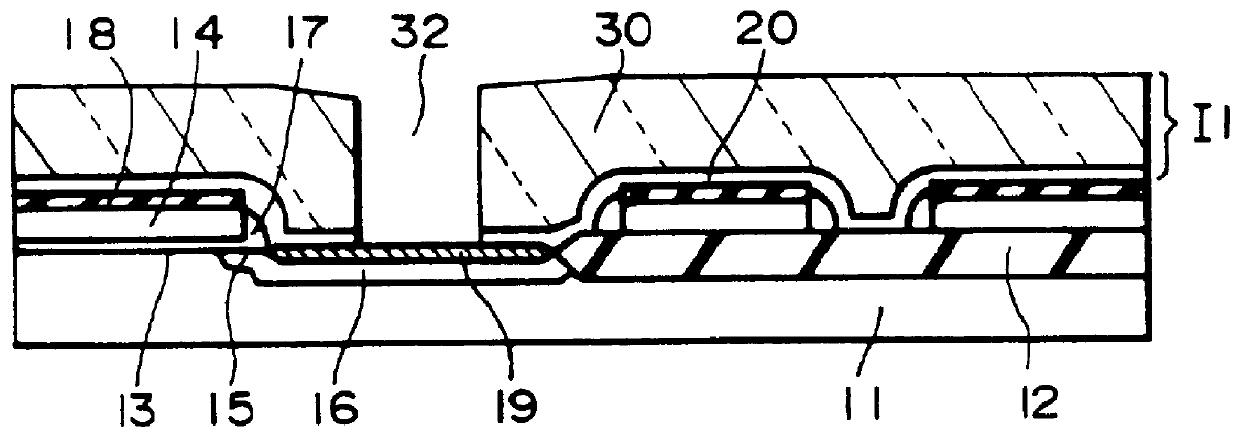
One feature of the method of fabricating a semiconductor device in the present invention is the inclusion of the step (b) of removing any gaseous components that may be contained within the interlayer dielectric (the degassing step), performed under specific conditions. The inclusion of this degassing step makes it possible to suppress the generation of gases such as water vapor, nitrogen, hydrogen, or oxygen that may be contained within the interlayer dielectric, during subsequent steps such as the formation of the second aluminum layer under high-temperature conditions of 300.degree. C. or higher. Although there are no specific limitations to the preparation of the interlayer dielectric, a chemical vapor deposition (CVD) film using tetraethoxysilane (TEOS) as a silane compound, a multi-layered film comprising a CVD film of TEOS, spin-on-glass (SOG) coatings and TEOS-CVD films, a silicon oxide film prepared by a polycondensation reaction of a silicon compound and hydrogen peroxide, and the like can be mentioned by way of examples.
Further, the steps (d), (e), and (f) are preferably performed sequentially within the same apparatus having a plurality of chambers and being maintained under a reduced pressure. This helps reduce the number of substrate movements and setting steps, thus simplifying the process and preventing substrate contamination.

Problems solved by technology

Filling such connection through-holes with wiring materials is very difficult and, therefore, has become an important technical challenge in recent years.
However, this has not improved far enough the problem of discontinuity that occurs at conductive parts within the connection through-holes due to causes such as voids.
In addition, these gases will be desorbed from the barrier layer and will exit from the interface with the aluminum layer during the formation of the aluminum layer, which will adversely affect the adhesiveness and fluidity of the aluminum layer.
However, if the chamber pressure is raised for cooling efficiency, the quantity of gas molecules within the chamber will increase proportionately, inviting a situation where the upper surface of the wafer is prone to contamination by the gas molecules.
This adversely affects the reflow of aluminum and can also lead to generation of voids as well as an increase in the wiring resistance.
Conversely, if the chamber pressure is reduced to prevent contamination of the wafer, the pressure in the space between the wafer and the stage will drop, lowering the thermal conductance between the wafer and the stage and, consequently, harming the cooling efficiency.
This ensures that the contamination of the upper surface of the wafer by gas molecules is prevented and, consequently, improves the reflow characteristics of the aluminum and reduces the resistance thereof.
If the power falls to zero, an oxide layer will form on the surface of the first aluminum layer even under reduced pressure, causing the wettability of the second aluminum layer to the first aluminum layer to deteriorate and the adhesiveness between them to worsen.
In addition, these gases will be desorbed from the wetting layer and will exit from the interface with the aluminum layer during the formation of the aluminum layer, which will adversely affect the adhesiveness and fluidity of the aluminum layer.
The upper end of the via-hole is then plugged by such a chemical compound or alloy to cause a condition called "pinch-off", which tends to hinder the aluminum flow into the via-hole, creating a void in the aluminum layer.

Method used


Image

  • Semiconductor device and method of fabricating the same
  • Semiconductor device and method of fabricating the same
  • Semiconductor device and method of fabricating the same

Examples


Embodiment Construction

>

(1) Experiments were performed to investigate differences in the quantity (partial pressure) of gases released from wafers when the second wiring region L2 is formed, both with and without the degassing step, with the results as shown in FIGS. 5 and 6.

In each of FIGS. 5 and 6, the horizontal axis represents the timing of steps from the heat treatment (heat treatment F) performed prior to the formation of the aluminum layers until after the formation of the second aluminum layer 65. The partial pressure of the gas remaining within the chamber is plotted along the vertical axis. In each of these graphs, the lines denoted by the reference letter A represent the results when the degassing step is performed after the formation of the second interlayer dielectric I2. The lines denoted by the reference letter B represent the results when no degassing step is performed after the formation of the second interlayer dielectric I2. In these experimental examples, the degassing step was perform...


PUM


Abstract

A semiconductor device having a contact structure that can exhibit superlative step coverage without causing voids or wiring discontinuities, using aluminum or aluminum alloys as a conductive substance for via-holes. A method of fabricating the semiconductor device comprises, for at least one layer of wiring regions above the first wiring region on a semiconductor substrate, the following steps (a) to (f): (a) a step of forming a via-hole in a second interlayer dielectric formed above the first wiring region on a semiconductor substrate; (b) a degassing step for removing gaseous components included within the interlayer dielectric by a heat treatment under reduced pressure and at the substrate temperature of 300 DEG C. to 550 DEG C.; (c) a step of forming a wetting layer on the surface of the interlayer dielectric and the via-hole; (d) a step of cooling the substrate to a temperature of no more than 100 DEG C.; (e) a step of forming a first aluminum layer comprising one of aluminum and an alloy in which aluminum is the main component on the wetting layer at a temperature of no more than 200 DEG C.; and (f) a step of forming a second aluminum layer comprising one of aluminum and an alloy in which aluminum is the main component on the first aluminum layer at a temperature of at least 300 DEG C.

Description

1. Field of the InventionThe present invention relates to a semiconductor device and a fabrication method therefor, and, in particular, to a semiconductor device that enables microminiaturization and has a contact structure using aluminum, and to a fabrication method therefor.2. Description of Background ArtIn a semiconductor device such as a LSI, recent advances in microminiaturization, integration, and multi-layering of elements have made it necessary to use connection through-holes such as contact holes and via-holes having high aspect ratios. Filling such connection through-holes with wiring materials is very difficult and, therefore, has become an important technical challenge in recent years. In this regard, attempts have been made to fill connection through-holes with aluminum or aluminum alloys that are useful as a wiring material.One of the techniques intended for the above requirement is disclosed, for example, in Japanese Patent Application Laid-Open No. 64-76736 / 1989. Th...

Claims


Application Information

Patent Timeline
IPC IPC(8): H01L21/02H01L21/70H01L21/768H01L21/285H01L21/203
CPCH01L21/28518H01L21/76801H01L21/76814H01L21/76828H01L21/76829H01L21/76834H01L21/76837H01L21/76843H01L21/76856H01L21/76876H01L21/76877H01L23/53223H01L21/28
Inventor ASAHINA, MICHIOTAKEUCHI, JUNICHIMORIYA, NAOHIROMATSUMOTO, KAZUKI
Owner SEIKO EPSON CORP
Learn More