
High energy density capacitor

a capacitor and high energy density technology, applied in the field of high energy density capacitors, can solve the problems of limited capacitors to low voltage applications, dielectric thickness limitations, and limitations of the skilled in the art when attempting to increase the energy density

Inactive Publication Date: 2000-07-25
SIGMA LAB OF ARIZONA
View PDF9 Cites 124 Cited by
  • Summary
  • Abstract
  • Description
  • Claims
  • Application Information

AI Technical Summary

Benefits of technology

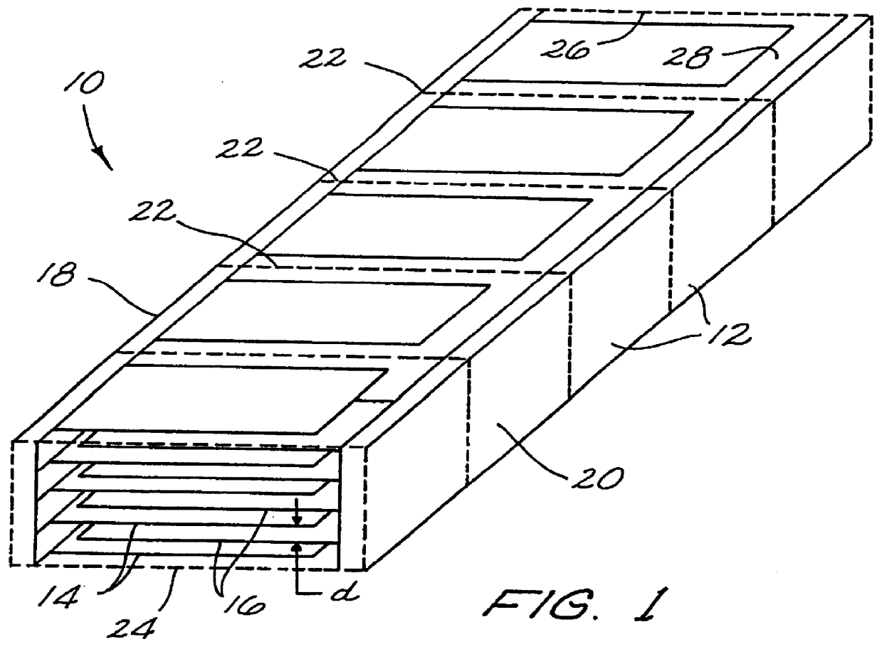
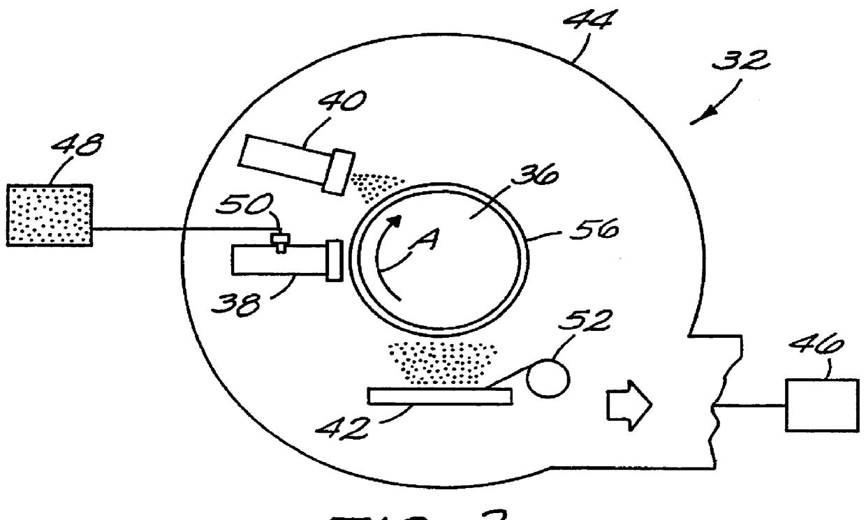
In accordance with the invention, a high energy density capacitor having an energy density of at least about 0.5 J / cm.sup.3 is provided. The capacitor comprises a plurality of interleaved, vacuum-deposited metal electrode layers separated by vacuum-deposited, radiation-cured polymer dielectric layers. The interleaved metal electrode layers terminate at opposite ends in a multilayer sputtered, solder-coated termination strip. The metal electrode layers are recessed into the polymer layers, thus creating a non-conducting region, to protect against arcing and leakage current between the metal electrode layers along the edges orthogonal to the solder terminations.
(c) the metal electrode layers within the polymer layer are recessed along edges orthogonal to the solder termination strips to prevent arcing between the metal electrode layers at the edges; and

Problems solved by technology

When designing high energy density capacitors with materials such as polypropylene (PP), polyester (PE), polycarbonate (PC), polyvinylidene fluoride (PVDE), and paper, the limitations that the person skilled in the art is faced with when attempting to increase the energy density include:
Dielectric thickness limitations due to mechanical strength of the self supported film.
These capacitors are limited to low voltage applications (<50V).

Method used


Image

  • High energy density capacitor
  • High energy density capacitor
  • High energy density capacitor

Examples


Embodiment Construction

A. Fundamental Considerations

The high energy density capacitor design of the present invention maximizes both .kappa. and E in Equation (1). The dielectric constant .kappa. is maximized by designing and synthesizing monomers tailored specifically to yield high dielectric constants. Monomers with dielectric constants up to 10 have been synthesized and tested, but it is expected that by use of the teachings herein, new monomers will be synthesized that yield dielectric constants above 10.

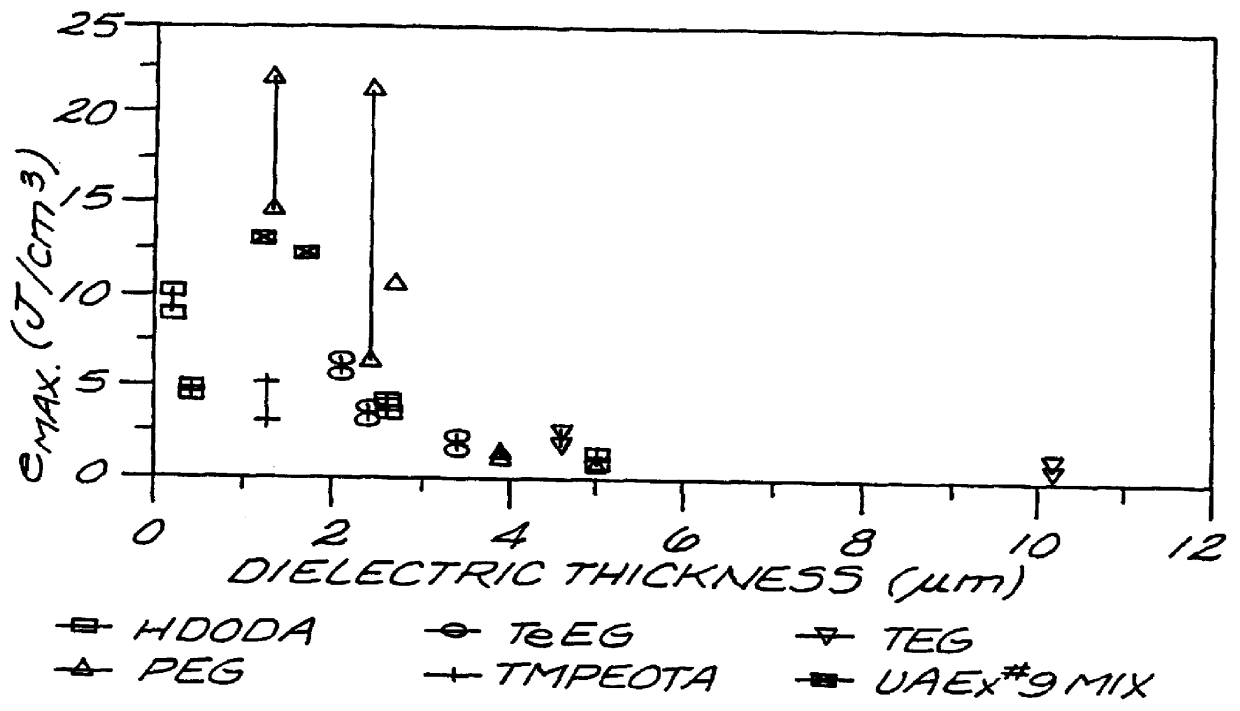
Because of the quadratic dependence of D on E, optimizing the maximum applied field has a greater effect than optimizing the dielectric constant. E.sub.m can be maximized by tailoring the polymer dielectric, by minimizing the thickness of the dielectric layer, and by limiting exposed edge breakdown. The PML technology is capable of producing ultra-thin polymer layers at an extremely high rate so that production speed is not compromised. The ultra-thin geometry maximizes the breakdown strength of the d...


PUM

PropertyMeasurementUnit
Forceaaaaaaaaaa
Sheet resistanceaaaaaaaaaa

Abstract

A high energy density, high power density capacitor having an energy density of at least about 0.5 J / cm3 is provided. The capacitor comprises a plurality of interleaved metal electrode layers separated by a polymer layer. The interleaved metal electrode layers terminate at opposite ends in a solder termination strip. The high energy density aspect of the capacitors of the invention is achieved by at least one of the following features: (a) the dielectric thickness between the interleaved metal electrode layers is a maximum of about 5 mu m; (b) the polymer is designed with a high dielectric constant kappa of at least about 3.5; (c) the metal electrode layers within the polymer layer are recessed along edges orthogonal to the solder termination strips to prevent arcing between the metal electrode layers at the edges; and (d) the resistivity of the metal electrode layers is within the range of about 10 to 500 ohms per square, or a corresponding thickness of about 200 to 30 ANGSTROM .

Description

The present invention relates generally to thin film capacitors, and, more particularly, monolithic multilayer, capacitors comprised of repeated layers of polymer dielectric and alternating metal electrodes. The polymer / metal multilayer is built up using a high speed vacuum deposition method according to which successive layers of radiation cured polymer dielectric and metal evaporated electrodes are deposited in a vacuum environment using a continuous and sequential deposition process.Metallized film capacitors are used extensively in a broad range of electrical and electronic equipment that include motor run and motor start circuits for air conditioners, fluorescent and high intensity light ballasts, power supplies, telecommunication equipment, instrumentation, and medical electronics. In many of these applications, the metallized capacitors are used to conserve energy by correcting the power factor of a circuit and in others they are used to perform specific functions, such as ti...

Claims


Application Information

Patent Timeline
IPC IPC(8): H01G4/18H01G4/30H01G4/14
CPCH01G4/18H01G4/30Y10T29/435
Inventor YIALIZIS, ANGELOMILLER, THEODORE A.
Owner SIGMA LAB OF ARIZONA
Learn More