Integrated circuit including vertical transistors with spacer gates having selected gate widths

a technology of integrated circuits and spacer gates, which is applied in the direction of transistors, electrical apparatus, semiconductor devices, etc., can solve the problems of design and manufacture of ever smaller and increased performance mosfets, and achieve the effects of improving integrated circuit density, compact structure, and small area

Inactive Publication Date: 2000-05-30
ADVANCED MICRO DEVICES INC +1
View PDF25 Cites 12 Cited by
  • Summary
  • Abstract
  • Description
  • Claims
  • Application Information

AI Technical Summary

Benefits of technology

Many advantages are gained by the described integrated circuit and fabrication method. The method advantageously forms a highly compact structure in which multiple transistors are formed in a very small area. The compact structure improves integrated circuit density and improves digital circuit performance. The fabrication method accurately, consistently, and highly controllably forms integrated circuit transistors and devices having channel widths that are substantially smaller than channel widths that are created using conventional photolithographic techniques.

Problems solved by technology

In fact, models of MOSFET functionality imply that the saturation drain current I.sub.dsat will continue to increase indefinitely as the channel length and gate oxide thickness are reduced so that only limitations of process technology rather than device effects prevent the design and manufacture of ever smaller and increased performance MOSFETs.

Method used


Image

  • Integrated circuit including vertical transistors with spacer gates having selected gate widths
  • Integrated circuit including vertical transistors with spacer gates having selected gate widths
  • Integrated circuit including vertical transistors with spacer gates having selected gate widths

Examples


second embodiment

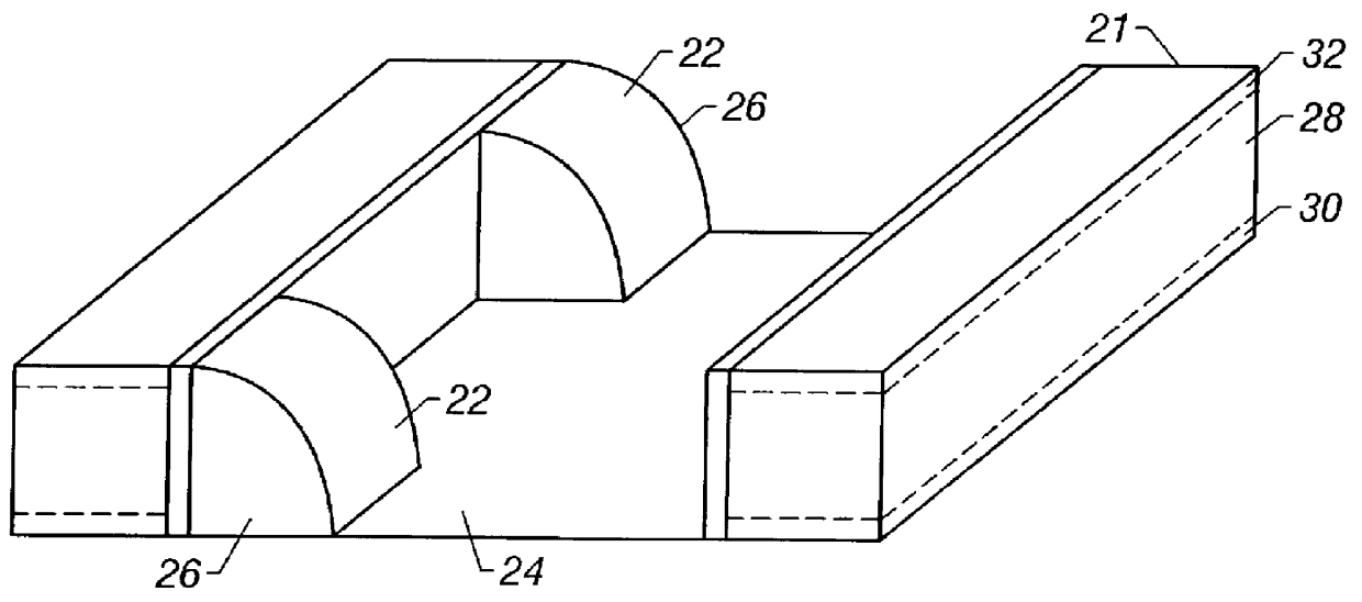
Referring to FIG. 2, a pictorial three-dimensional view shows an integrated circuit using a masking technique to form multiple spacer transistors with individually selected gate widths. A silicon wafer 21 includes a plurality of transistors 22 formed in a trench 24 etched into the wafer 21. A masking process is used to form transistors 22 on only one side of the trench 24. The transistors 22 include a polysilicon gate 26 which is formed from a sidewall spacer on the edges of the trench 4. The transistors 22 also include a channel region 28 extending vertically within the silicon wafer 21 on the sides of the trench 24, and a source region 30 and a drain region 32 bounding the channel region 28. The source region 30 and the drain region 32 overlie and underlie the channel region 28. The width of the channel region 28 determines the size of the transistors 22 and is selected within very compact ranges such as a range from 0.1 .mu.m to 0.3 .mu.m, advantageously forming a highly compact ...

third embodiment

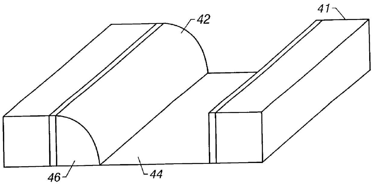
Referring to FIG. 3, a pictorial three-dimensional view shows an integrated circuit using a masking technique to form a polysilicon interconnect structure 42 connecting multiple devices on a semiconductor wafer 41. A silicon wafer 41 includes a plurality of devices (not shown) formed adjacent to a trench 44 etched into the wafer 41. The interconnect structure 42 is formed by depositing a blanket layer of undoped polysilicon by low pressure chemical vapor deposition (LPCVD) on the top surface of the silicon wafer 41. The undoped polysilicon is etched using an anisotropic dry etch process that is selective to polysilicon over SiO.sub.2 etching to avoid etching of underlying gate oxide. The anisotropic dry-etch process clears undoped polysilicon in planar areas of the surface regions and the floor of the trench 44 in the silicon wafer 41 while leaving the interconnect structure 42 on vertical sidewalls 46 of the trench 44. The interconnect structure 42 is etched to an endpoint with min...


PUM


Abstract

Improvements in the compactness and performance of integrated circuit devices are gained through the fabrication of vertical transistors for which channel sizes are determined by the accuracy of etch techniques rather than the resolution of photolithographic techniques. A method of fabricating an integrated circuit includes forming a plurality of doped layers in a series of depths in a substrate wafer, and etching a trench in the substrate wafer. The trench extends through the doped layers at a plurality of depths and is bounded by vertical sidewalls and a planar horizontal floor. The method further includes forming a conductive sidewall spacer adjacent to the vertical sidewalls of the trench.

Description

1. Field of the InventionThe present invention relates to an integrated circuit and fabrication method. More specifically, the present invention relates to an integrated circuit including vertical transistors with spacer gates.2. Description of the Related ArtA key concept in the evolution of MOSFET integrated circuits is the usage of scaling to continually reduce the size of devices and thereby increase the density and speed of digital integrated circuits. The density of integrated circuits is improved by using smaller channel lengths and channel widths. The speed of digital integrated circuits is improved by increasing the saturation drain current I.sub.dsat of MOSFET devices, thereby promoting faster charging and discharging of parasitic capacitances. Fortunately, an increase in the saturation drain current I.sub.dsat of MOSFET devices automatically results from a decrease in channel length or a reduction in gate oxide thickness. In fact, models of MOSFET functionality imply that...

Claims


Application Information

Patent Timeline
Patent Type & Authority Patents(United States)
IPC IPC(8): H01L21/02H01L21/336H01L29/66H01L21/70H01L29/78H01L21/8234H01L27/085H01L27/088
CPCH01L21/823468H01L21/823487H01L29/7827H01L29/66666H01L27/088
Inventor HAUSE, FREDERICK N.GARDNER, MARK I.
Owner ADVANCED MICRO DEVICES INC
Why Eureka
Try Eureka