Method of manufacturing semiconductor device

Pending Publication Date: 2022-09-29
MITSUBISHI ELECTRIC CORP
View PDF0 Cites 0 Cited by
  • Summary
  • Abstract
  • Description
  • Claims
  • Application Information

AI Technical Summary

Benefits of technology

This patent is about reducing the number of masks used to create impurities in a semiconductor device with a trench-type MOS gate structure. The method involves using an ion implantation process to first form a base layer and then add the impurities to the semiconductor substrate before creating the trench gates. This method reduces the number of masks needed and also helps to maintain a consistent impurity profile, which helps to improve the overall performance of the semiconductor device.

Problems solved by technology

There has been a problem of high manufacturing cost due to the three impurity layers because different masks are used for forming the three respective layers.
The problem occurs not only in a trench gate type IGBT but also in other semiconductor devices having a trench type MOS gate structure.
According to the manufacturing method proposed in Japanese Patent Application Laid-Open No. 2016-046445, there has been a problem in that, the impurity layer is formed by oblique implantation after the trench gates are formed; therefore, the profile of the impurity layer varies due to the influence of steps on the surface of the semiconductor substrate.

Method used


Image

  • Method of manufacturing semiconductor device
  • Method of manufacturing semiconductor device
  • Method of manufacturing semiconductor device

Examples


embodiment 1

A. Embodiment 1

[0035]

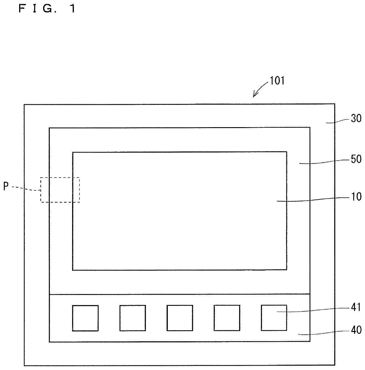
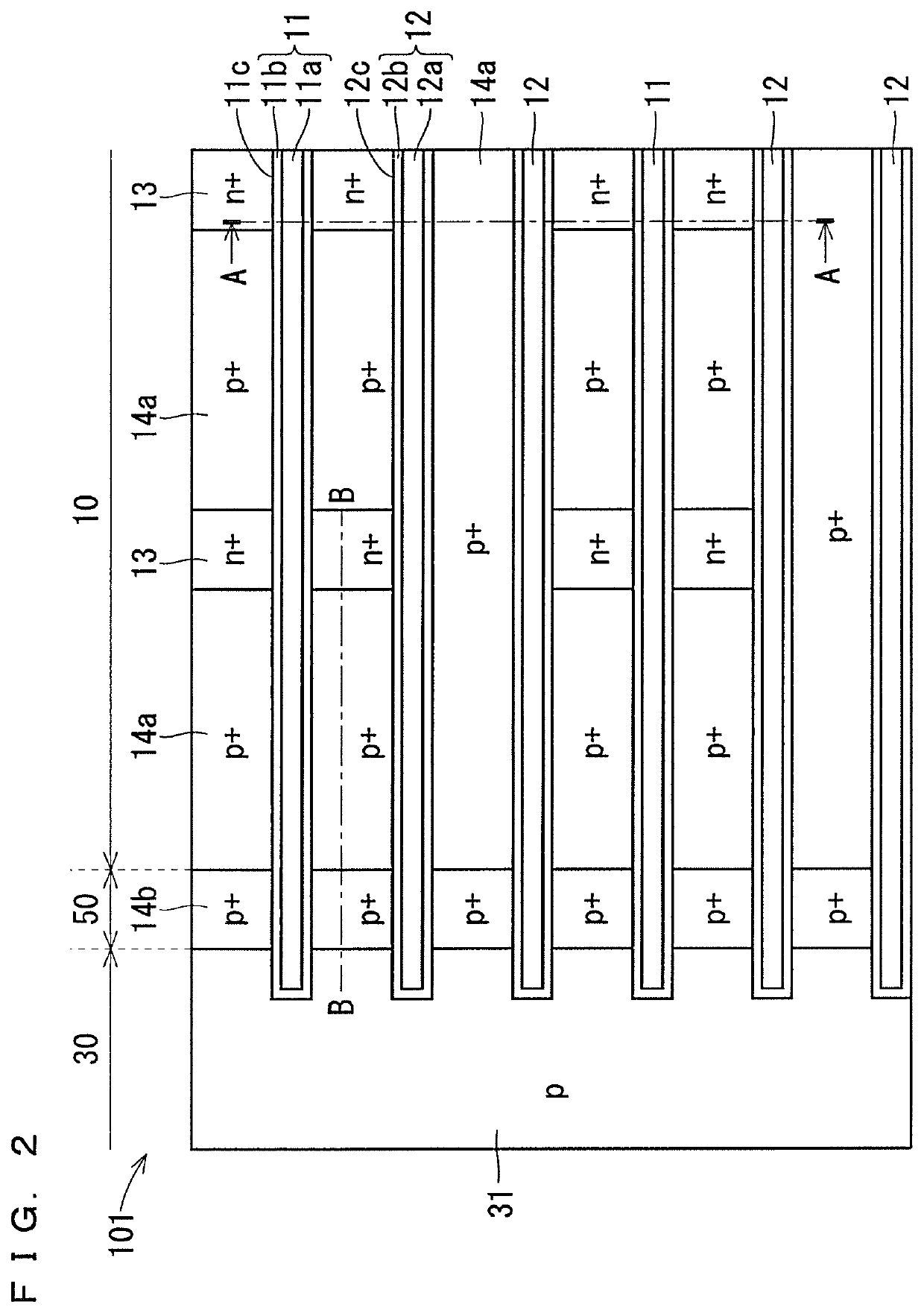
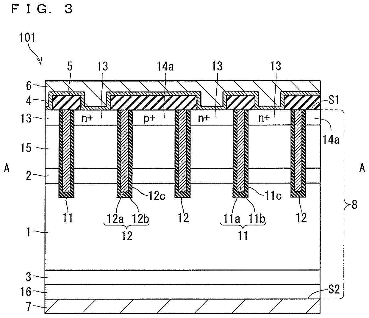
[0036]FIG. 1 is a plan view of an IGBT 101 being a semiconductor device of Embodiment 1. FIG. 2 is an enlarged plan view of a region P illustrated in FIG. 1 of the IGBT 101. FIG. 3 is a cross-sectional view of the IGBT 101 along the line A-A of FIG. 2. FIG. 4 is a cross-sectional view of the IGBT 101 along the line B-B of FIG. 2.

[0037]First, the planar structure of the IGBT 101 will be described. As illustrated in FIG. 1, the IGBT 101 includes an active region 10, a boundary region 50, and an edge region 30. That is, the IGBT 101 is demarcated into the active region 10, the boundary region 50, and the edge region 30 in plan view. The boundary region 50 surrounds the active region 10 in plan view. The edge region 30 surrounds the boundary region 50 in plan view. A pad region 40 including pads 41 may be provided between the boundary region 50 and the edge region 30 in plan view.

[0038]Next, with reference to FIG. 4, the cross-sectional structure of the IGBT 101 com...

embodiment 2

B. Embodiment 2

[0069]

[0070]FIG. 11 is a cross-sectional view of an IGBT 102 of Embodiment 2 along the line B-B of FIG. 2. Other cross-sectional configurations and planar configurations of the IGBT 102 are the same as those of the IGBT 101 of Embodiment 1.

[0071]In the IGBT 102, the width Wi of the boundary region 50 is greater than the depth De of the emitter layer 13. Further, in the IGBT 102, the depth Dh of the first contact layer 14a and the second contact layer 14b is deeper than the depth De of the emitter layer 13.

[0072]

[0073]In the IGBT 102 of Embodiment 2, the width Wi of the boundary region 50 is greater than the depth De of the emitter layer 13. Therefore, the n-type impurity ions implanted to form the emitter layer 13 do not reach the edge region 30 even if the semiconductor substrate 8 is diffused in the lateral direction. As a result, the formation of the parasitic emitter layer on the surface of the edge region 30 is suppressed, and improvement in the fracture resistan...

embodiment 3

C. Embodiment 3

[0075]

[0076]FIG. 13 is an enlarged plan view of the IGBT 102 of Embodiment 2 in the region P of FIG. 1. FIG. 14 is a cross-sectional view of the IGBT 103 along the line C-C of FIG. 13. As illustrated in FIGS. 13 and 14, the IGBT 103 has a p-type third contact layer 14c interposed between the first contact layers 14a on both sides in the active region 10 and is otherwise similar to the IGBT 101.

[0077]The third contact layer 14c does not contain n-type impurities having a concentration equal to or higher than the n-type impurity concentration of the drift layer 1. The net impurity concentration of the third contact layer 14c is higher than the net impurity concentration of the first contact layer 14a. In FIG. 14, although the base layer 15 and the carrier storage layer 2 immediately below the third contact layer 14c are locally shallow, the base layer 15 and the carrier storage layer 2 may be uniformly formed as in the IGBT 101 of Embodiment 1.

[0078]The base layer 15 an...


PUM


Abstract

An object of the present disclosure is to reduce masks and to reduce the variation in the profile of an impurity layer in a semiconductor device. A method of manufacturing a semiconductor device includes a step (b) of forming a base layer on a first main surface side of a drift layer in an active region by implanting p-type impurity ions of using the first mask, a step of (c) of forming an emitter layer on the first main surface side of the base layer by implanting n-type impurity ions using the first mask, a step (d) of forming trenches after the steps (b) and (c), a step (e) of embedding a gate electrode inside the trenches, and a step (g) of converting a part of the emitter layer into a first contact layer by implanting the p-type impurity ions having a high dosage using a second mask.

Description

BACKGROUND OF THE INVENTIONField of the Invention[0001]The present disclosure relates to a method of manufacturing a semiconductor device.Description of the Background Art[0002]From the viewpoint of energy saving, IGBTs or diodes are used in power modules and the like for variable speed control of three-phase motors in the fields of general-purpose inverters and AC servo motors. In order to reduce inverter loss, IGBTs or diodes are required to have devices with low switching loss and low on-voltage.[0003]As a device having a low switching loss, a trench gate type IGBT represents thereof. An N-channel trench gate type IGBT has three impurity layers: a P-type base layer, an N-type emitter layer, and a P-type contact layer. There has been a problem of high manufacturing cost due to the three impurity layers because different masks are used for forming the three respective layers. The problem occurs not only in a trench gate type IGBT but also in other semiconductor devices having a tre...

Claims


Application Information

Patent Timeline
IPC IPC(8): H01L21/266H01L21/768H01L21/22
CPCH01L21/266H01L21/76831H01L21/2225H01L29/66666H01L29/401H01L21/2253H01L29/7397H01L29/0696H01L29/66348H01L29/407H01L29/1095
Inventor NISHI, KOICHISONEDA, SHINYAKONISHI, KAZUYA
Owner MITSUBISHI ELECTRIC CORP
Why Eureka
Try Eureka