Optical alignment systems and methods using silicon diodes

a technology of optical alignment and silicon diodes, applied in the field of optical alignment systems and methods of lasers, can solve the problem of not intended summary, and achieve the effect of reducing manufacturing costs, simplifying the design of silicon photonics chips, and miniaturizing the overall size of integrated photonic chips

Pending Publication Date: 2022-08-11
ALPINE OPTOELECTRONICS INC
View PDF0 Cites 0 Cited by
  • Summary
  • Abstract
  • Description
  • Claims
  • Application Information

AI Technical Summary

Benefits of technology

[0009]In an aspect, an integrated photonics chip is provided. The integrated photonics chip may comprise: a plurality of optical channels extending a length of the integrated photonics chip; at least one variable optical attenuator (VOA) being optically connected to one of the plurality of optical channels, the at least one VOA comprising a silicon diode; at least one modulator being optically connected to another of the plurality of optical channels, the at least one modulator comprising a silicon diode; wherein the silicon diodes of the at least one VOA and the at least one modulator are adapted to receive biasing voltages; and wherein an application of the biasing voltages causes the silicon diodes of the at least one VOA and the at least one modulator to be reverse-biased, such that the at least one VOA is adapted to detect a photocurrent of a first optical signal being propagated along the one of the plurality of optical channels, and the at least one modulator is adapted to detect a photocurrent of a second optical signal being propagated along the another of the plurality of optical channels. Thus, an advantage of using silicon-based modulators and VOAs is that the use of additional on-chip tap couplers bundled with photodiodes may be negated, which simplifies the design of the disclosed silicon photonics chip, and thus reduces manufacturing costs. Another advantage is that, because the use of additional on-chip tap couplers bundled with photodiodes may be negated, the overall size of the integrated photonics chip may be miniaturized, further reducing manufacturing costs. An additional advantage is that, because no electrical power is needed for operating the negated on-chip photodiodes, the operational costs associated with operating the disclosed integrated photonics chip may be reduced. Another advantage is that, because no tap couplers are used, the wavelength dispersion of the propagating laser light may be improved. Another advantage is that, because no SiGe photodiodes are used, the typical issues of high ESD sensitivity and specificity of the SiGe epitaxial growth yield may be avoided.
[0010]In another aspect, a method of optically aligning a laser light source to an integrated photonics chip is provided, the integrated photonics chip comprising a first and a second optical channels, and a first and a second variable optical attenuators (VOAs) being optically connected to the first and the second optical channels, respectively, the first and the second VOAs each having a silicon diode, wherein the silicon diodes of the first VOA and the second VOA are each adapted to receive a first and a second biasing voltages, respectively. The method may comprise the steps of: positioning the laser source to face a first end of the integrated photonics chip, such that an optical signal being launched by the laser source can enter the integrated photonics chip at the first end; applying the first and the second biasing voltages to each of the silicon diodes of the first and the second VOAs, the first and the second biasing voltages causing the silicon diodes to become reverse-biased, such that a photocurrent of a propagating optical signal can be detected by each of the first and the second VOAs; operating the laser source, such that a first and a second optical signals are launched into the first and the second optical channels, respectively, at the first end; and measuring an optical power of each of the first and the second optical signals by detecting the photocurrent of each of the first and the second optical signals, respectively, using the reverse-biased first and second VOAs, such that to monitor and thus selectively adjust a position of the laser source and an angle of incidence of each of the first and the second optical signals for optically aligning the laser source to the integrated photonics chip. Thus, an advantage is that the required number of on-chip optical components is simplified and thus reduced, increasing chip optimization and circuit miniaturization. An additional advantage of the disclosed optical alignment method using reverse-biased VOAs and modulators is that a laser source may be efficiently and cost-effectively aligned to an integrated photonics die. Another advantage of the disclosed optical alignment method is that a laser source may be aligned to an integrated photonics die using existing, on-chip optical components, thus reducing operational costs.
[0011]In another aspect, a method of optically aligning a laser light source to an integrated photonics chip is provided, the integrated photonics chip comprising a first and a second optical channels, and a first and a second modulators being optically connected to the first and the second optical channels, respectively, the first and the second modulators each having a silicon diode, wherein the silicon diodes of the first and the second modulators are each adapted to receive a first and a second biasing voltages, respectively. The method may comprise the steps of: positioning the laser source to face a first end of the integrated photonics chip, such that an optical signal being launched by the laser source can enter the integrated photonics chip at the first end; applying the first and the second biasing voltages to each of the silicon diodes of the first and the second modulators, respectively, the first and the second biasing voltages causing the silicon diodes to become reverse-biased, such that a photocurrent of a propagating optical signal can be detected by each of the first and the second modulators; operating the laser source, such that a first and a second optical signals are launched into the first and the second optical channels, respectively, at the first end; and measuring an optical power of each of the first and the second optical signals by detecting a photocurrent of each of the first and the second optical signals, respectively, using the reverse-biased first and second modulators, such that to monitor and thus selectively adjust a position of the laser source and an angle of incidence of each of the first and the second optical signals for optically aligning the laser source to the integrated photonics chip. Thus, an advantage is that the required number of on-chip optical components is simplified and thus reduced, increasing chip optimization and circuit miniaturization. An additional advantage of the disclosed optical alignment method using reverse-biased VOAs and modulators is that a laser source may be efficiently and cost-effectively aligned to an integrated photonics die. Another advantage of the disclosed optical alignment method is that a laser source may be aligned to an integrated photonics die using existing, on-chip optical components, thus reducing operational costs.

Problems solved by technology

Moreover, this Summary is not intended for use as an aid in determining the scope of the claimed subject matter.

Method used


Image

  • Optical alignment systems and methods using silicon diodes
  • Optical alignment systems and methods using silicon diodes
  • Optical alignment systems and methods using silicon diodes

Examples


Embodiment Construction

[0020]What follows is a description of various aspects, embodiments and / or examples in which the invention may be practiced. Reference will be made to the attached drawings, and the information included in the drawings is part of this detailed description. The aspects, embodiments and / or examples described herein are presented for exemplification purposes, and not for limitation purposes. It should be understood that structural and / or logical modifications could be made by someone of ordinary skills in the art without departing from the scope of the invention. Therefore, the scope of the invention is defined by the accompanying claims and their equivalents.

[0021]It should be understood that, for clarity of the drawings and of the specification, some or all details about some structural components or steps that are known in the art are not shown or described if they are not necessary for the invention to be understood by one of ordinary skills in the art.

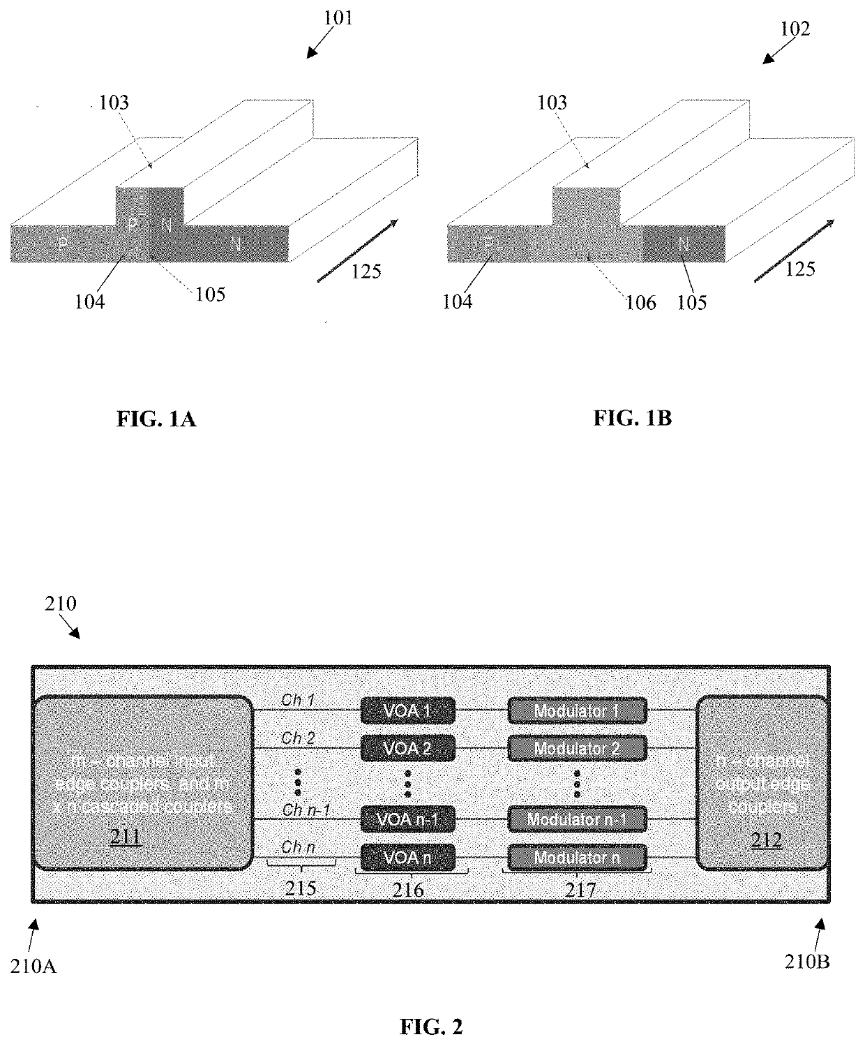
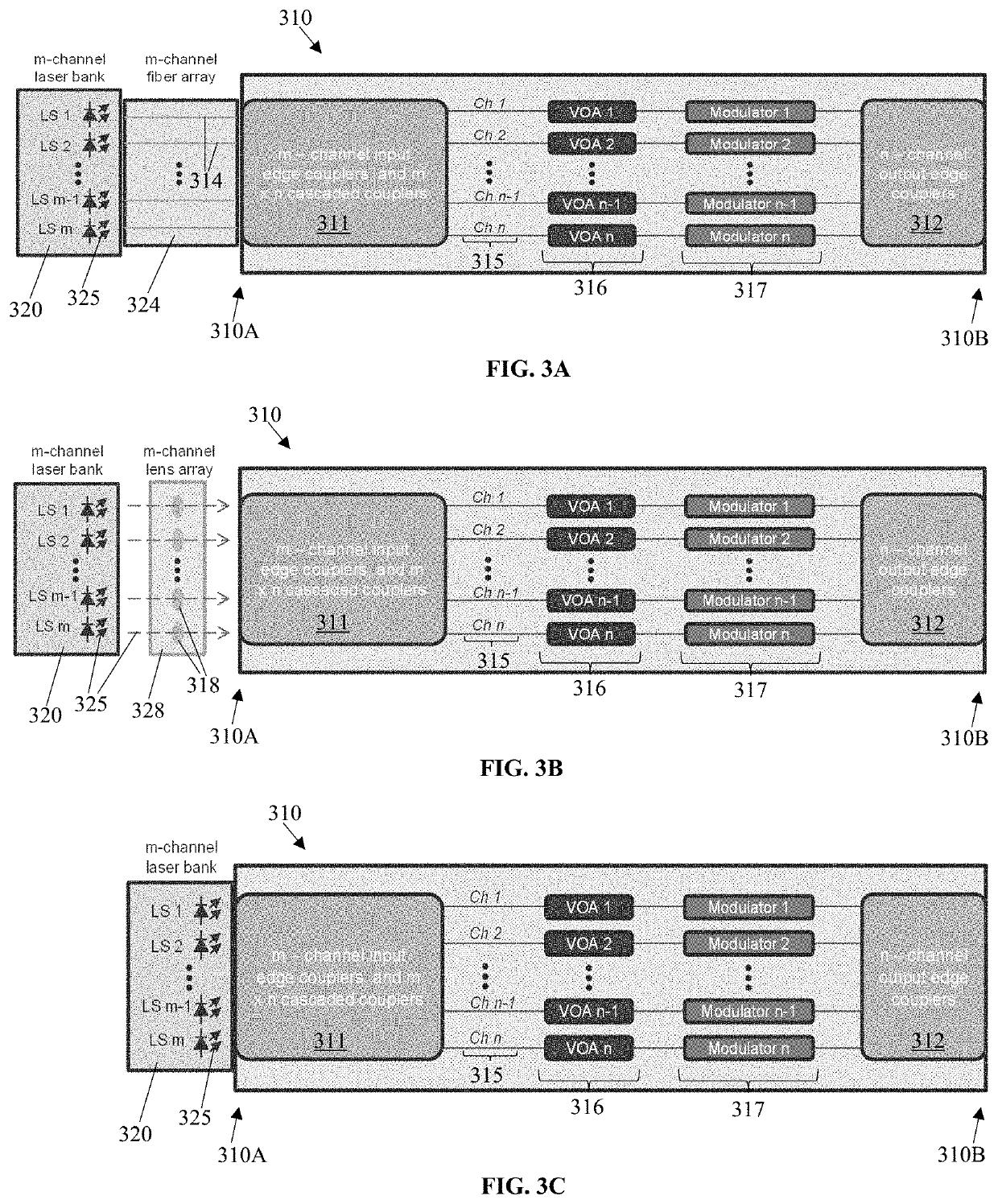
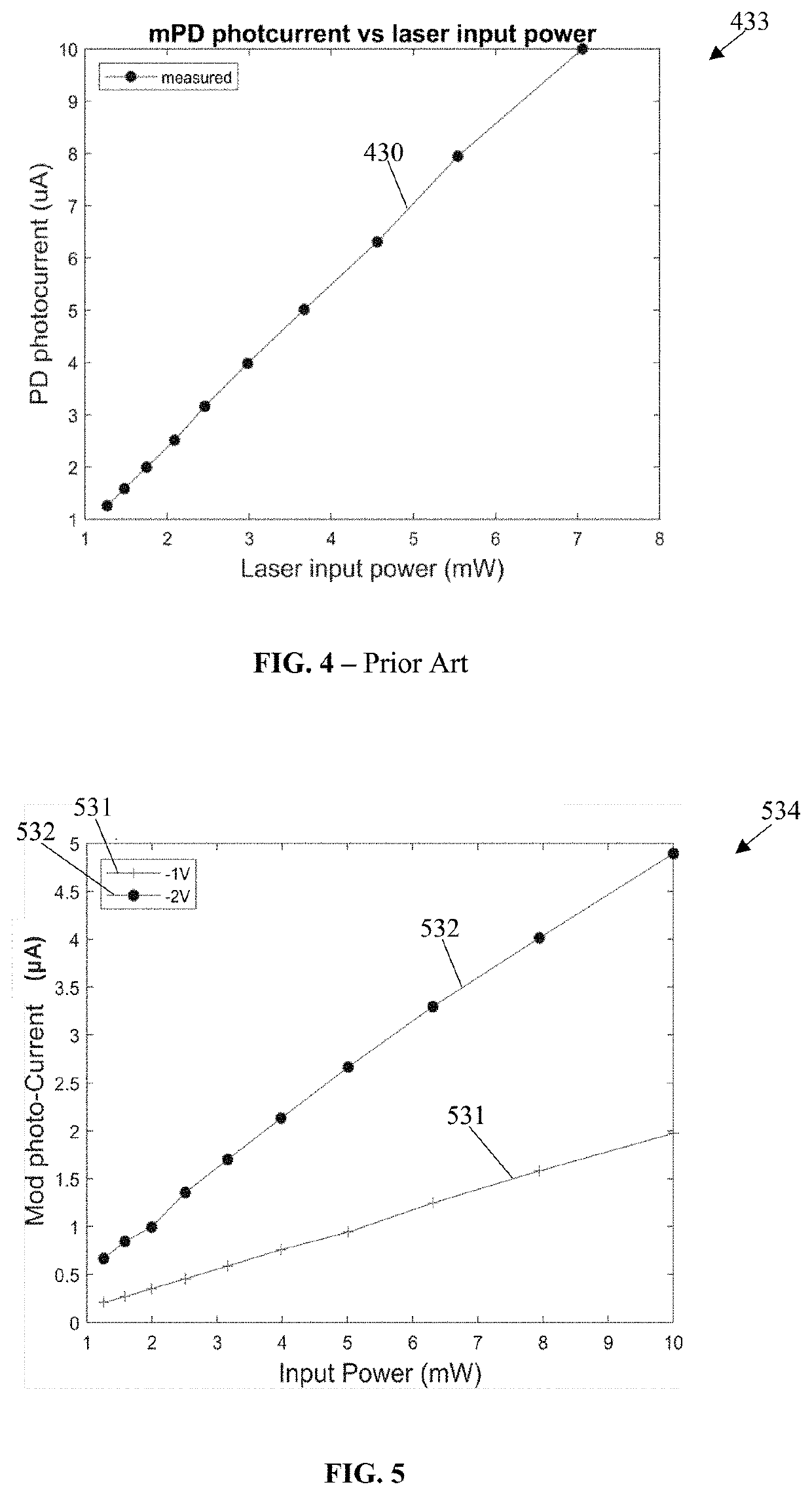
[0022]For the following descr...


PUM

PropertyMeasurementUnit
biasing voltagesaaaaaaaaaa

Abstract

An integrated photonics chip comprising: a plurality of optical channels extending a length of the integrated photonics chip; at least one variable optical attenuator (VOA) being optically connected to one of the plurality of optical channels, the at least one VOA comprising a silicon diode; at least one modulator being optically connected to another of the plurality of optical channels, the at least one modulator comprising a silicon diode; wherein the silicon diodes of the at least one VOA and the at least one modulator are adapted to receive biasing voltages; and wherein an application of the biasing voltages causes the silicon diodes of the at least one VOA and the at least one modulator to be reverse-biased, such that the at least one VOA and the at least one modulator are each adapted to detect a photocurrent of an optical signal being propagated along the plurality of optical channels.

Description

BACKGROUND OF INVENTION1. Field of the Invention[0001]The invention relates generally to systems and methods of optically aligning lasers to integrated photonics chips, and more specifically to systems and methods of optically aligning lasers to integrated photonics chips using reverse-biased silicon diodes.2. Description of the Related Art[0002]Over the last twenty years or so, silicon photonics technology has gained significant progress in the field of integrated photonics, making silicon photonics a competitive technology platform for the most modern and state-of-the-art optical communication applications. In optical communications, for example, an optical transmitter and optical receiver pair is needed (at minimum) to optically transmit and receive information and data signals (in the form of light signals, for example). To achieve a high data rate, and over a distance longer than 100 meters (m), an optical transmitter would conventionally include at least a continuous wave or t...

Claims


Application Information

Patent Timeline
Patent Type & Authority Applications(United States)
IPC IPC(8): G02F1/01H01S5/00H01S5/02251H01S5/02253H01S5/40H01L27/144
CPCG02F1/0123H01S5/0085H01S5/02251G02F2203/48H01S5/0071H01S5/4087H01L27/1443H01S5/02253H01S5/0225H01S5/02326
Inventor ZHENG, DAWEIZHANG, XINGYUWANG, TONGQING
Owner ALPINE OPTOELECTRONICS INC
Why Eureka
Try Eureka