Wafer producing method

Pending Publication Date: 2022-05-12
DISCO CORP
View PDF0 Cites 0 Cited by
  • Summary
  • Abstract
  • Description
  • Claims
  • Application Information

AI Technical Summary

Benefits of technology

The present invention is a method for producing wafers that can reduce the chance of chipping occurring in the wound edge of the wafer during post-processing. This is achieved by applying a laser beam only to the central region of the workpiece, leaving the peripheral region unchanged. This method prevents the formation of ablation traces on the outer edge of the wafer and reduces the likelihood of chipping occurring.

Problems solved by technology

Here, the power of the laser beam at the condensing point may not be stable when the vicinity of one end and the vicinity of another end (peripheral region) of the ingot are irradiated with the laser beam.

Method used


Image

  • Wafer producing method
  • Wafer producing method
  • Wafer producing method

Examples


Embodiment Construction

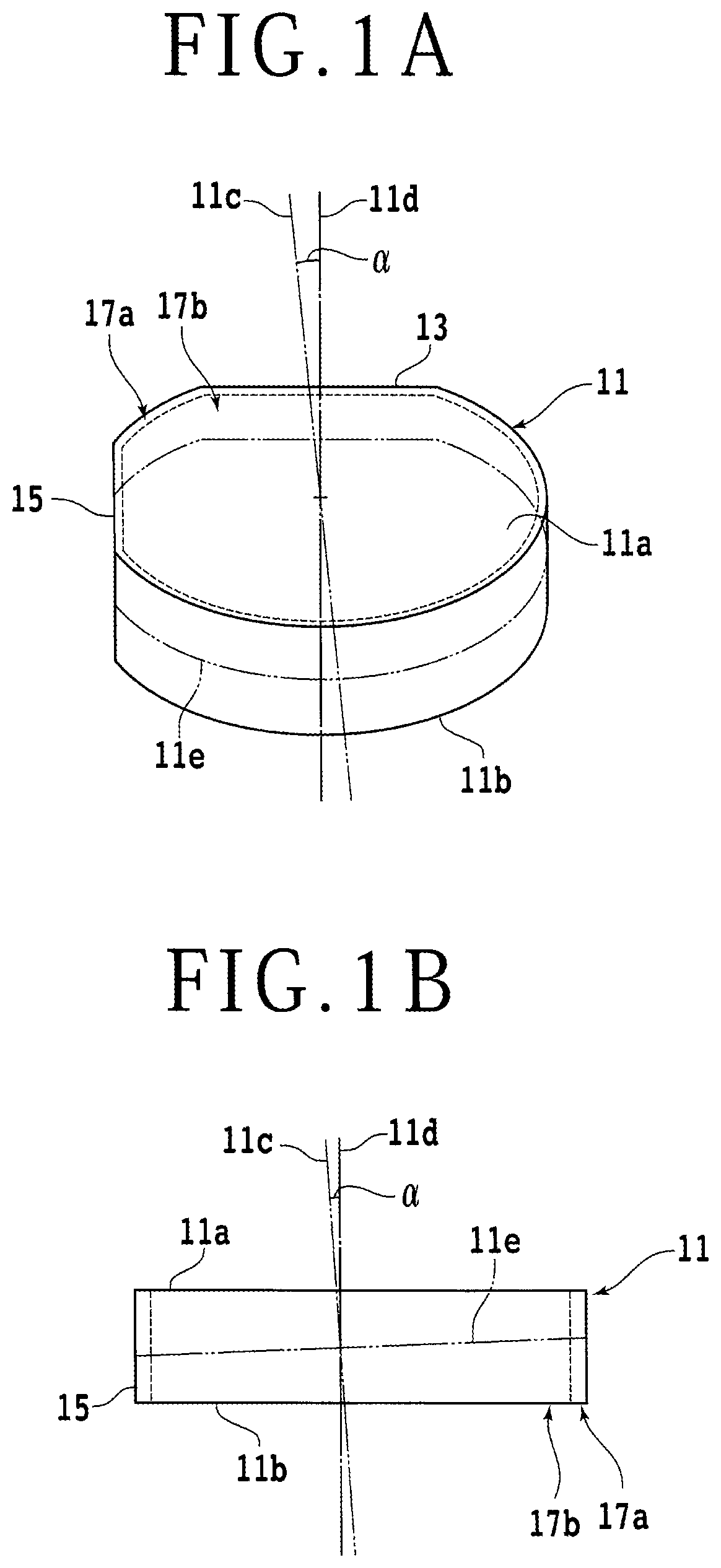
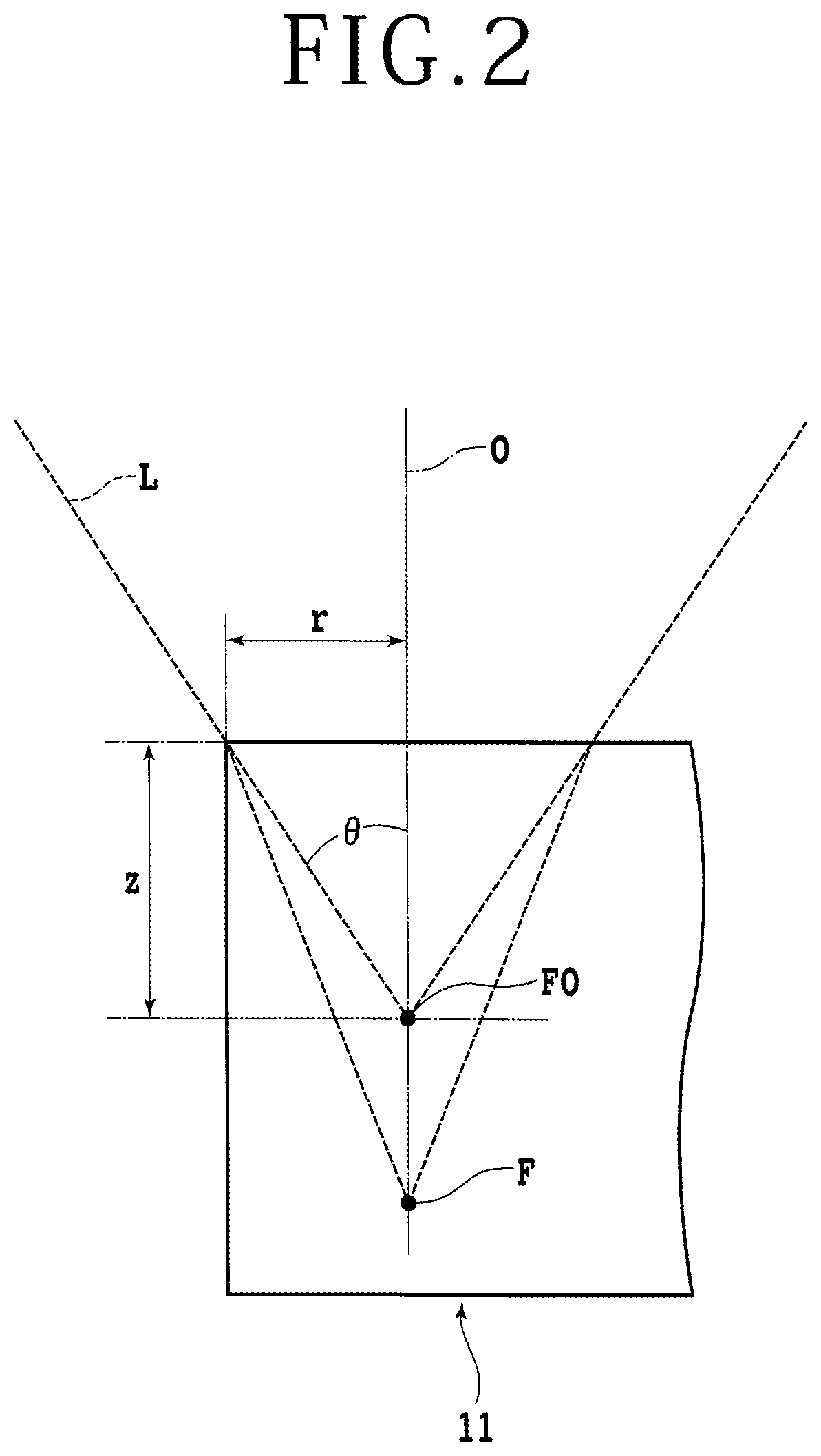
[0041]An embodiment of the present invention will be described with reference to the accompanying drawings. FIG. 1A is a perspective view schematically illustrating an example of a workpiece used in a wafer producing method according to the present embodiment. FIG. 1B is a side view schematically illustrating an example of the workpiece. The workpiece 11 illustrated in FIG. 1A and FIG. 1B is a cylindrical single crystal SiC ingot having a top surface (first surface) 11a and an undersurface (second surface) 11b substantially parallel with each other.

[0042]The workpiece 11 is produced by using epitaxial growth. Then, the workpiece 11 is produced such that a c-axis 11c of single crystal SiC is slightly inclined with respect to a normal 11d to the top surface 11a and the undersurface 11b in order to reduce lattice defects formed internally. For example, an angle (off angle) a formed between the c-axis 11c and the normal 11d is 1° to 6° (typically 4°).

[0043]Two flat portions indicating t...


PUM

PropertyMeasurementUnit
Distanceaaaaaaaaaa

Abstract

A peeling layer is formed by applying a laser beam only to a central region of a workpiece other than a peripheral region extending inward from the peripheral edge of the workpiece by a predetermined distance. In this case, the application of the laser beam does not form the peeling layer in the peripheral region of the workpiece, and the formation of an ablation trace on the outer peripheral surface of the workpiece is prevented. As a result, it is possible to reduce a probability of occurrence of chipping in the peripheral region of a wafer peeled off from the workpiece when the wafer is subjected to a post-process.

Description

BACKGROUND OF THE INVENTIONField of the Invention[0001]The present invention relates to a wafer producing method.Description of the Related Art[0002]Chips of semiconductor devices are generally manufactured by using a disk-shaped wafer. This wafer is, for example, cut out from a cylindrical semiconductor ingot by using a wire saw, and thereafter produced by polishing the top surface of the wafer and thus finishing the top surface into a mirror surface (see Japanese Patent Laid-Open No. 2000-94221, for example).[0003]Specifically, when the wafer is cut out from the ingot by using the wire saw, minute irregularities are formed on the top surface of the wafer, and the wafer is curved as a whole (a warp occurs in the wafer). Therefore, the top surface of the wafer thus cut out is often polished in order to planarize the wafer by removing the irregularities.[0004]However, when the wafer is polished, a part of the polished surface side of the wafer becomes a polishing swarf and is discard...

Claims


Application Information

Patent Timeline
IPC IPC(8): H01L21/304H01L21/04B23K26/53B23K26/38H01L21/67
CPCH01L21/3043H01L21/0445B23K2101/40B23K26/38H01L21/67092B23K26/53B23K26/36B23K26/362H01L21/02013H01L21/02021H01L21/0201B23K2103/50B23K26/032B23K26/3576
Inventor HIRATA, KAZUYA
Owner DISCO CORP
Why Eureka
Try Eureka