CF on TFT liquid crystal display having reduced dot defects

Inactive Publication Date: 2005-02-08
VISTA PEAK VENTURES LLC
View PDF15 Cites 6 Cited by
  • Summary
  • Abstract
  • Description
  • Claims
  • Application Information

AI Technical Summary

Benefits of technology

Therefore, it is an object of the present invention to provide a liquid crystal display and a manufacturing method thereof in which a probability of occurrence of dot defects can be greatly reduced.
It is another object of the present invention to provide a CF on TFT type liquid crystal display which has high resolution and in which a probability of occurrence of dot defects can be greatly reduced and to provide a manufacturing method of such liquid crystal display.
It is still another object of the present invention to provide a CF on TFT type liquid crystal display and a manufacturing method thereof in which reliability and completeness of contact between drain electrodes or drain signal lines and pixel electrodes can be greatly improved.

Problems solved by technology

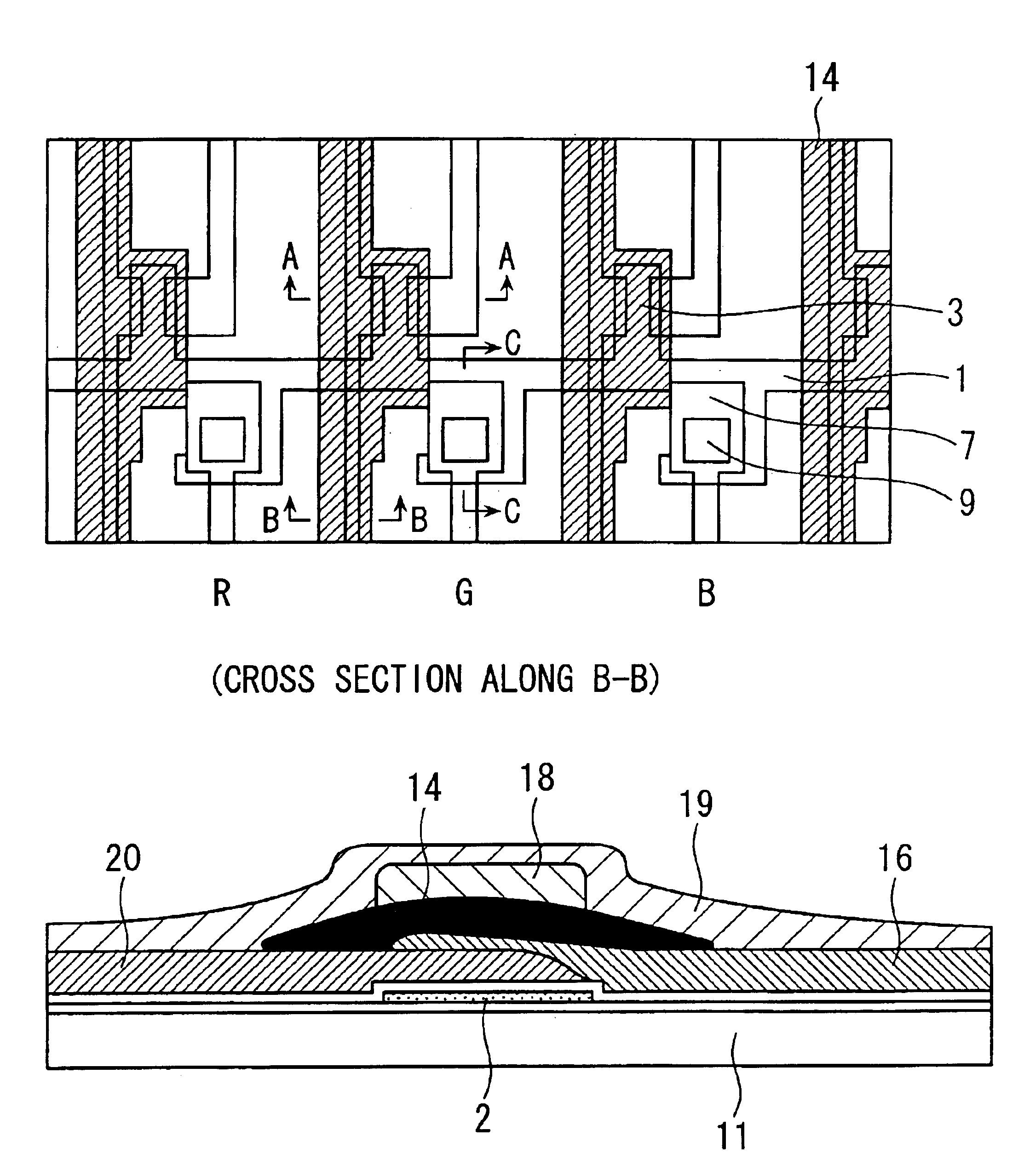
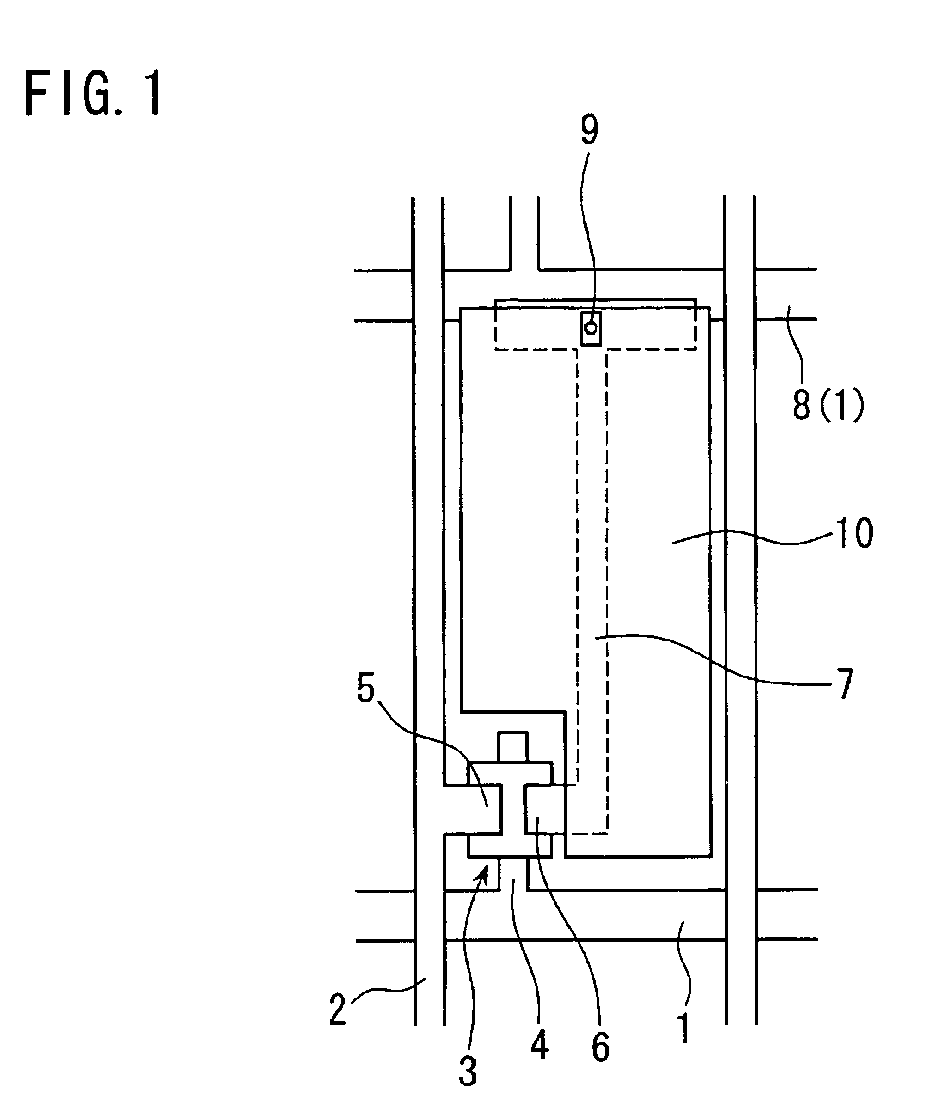
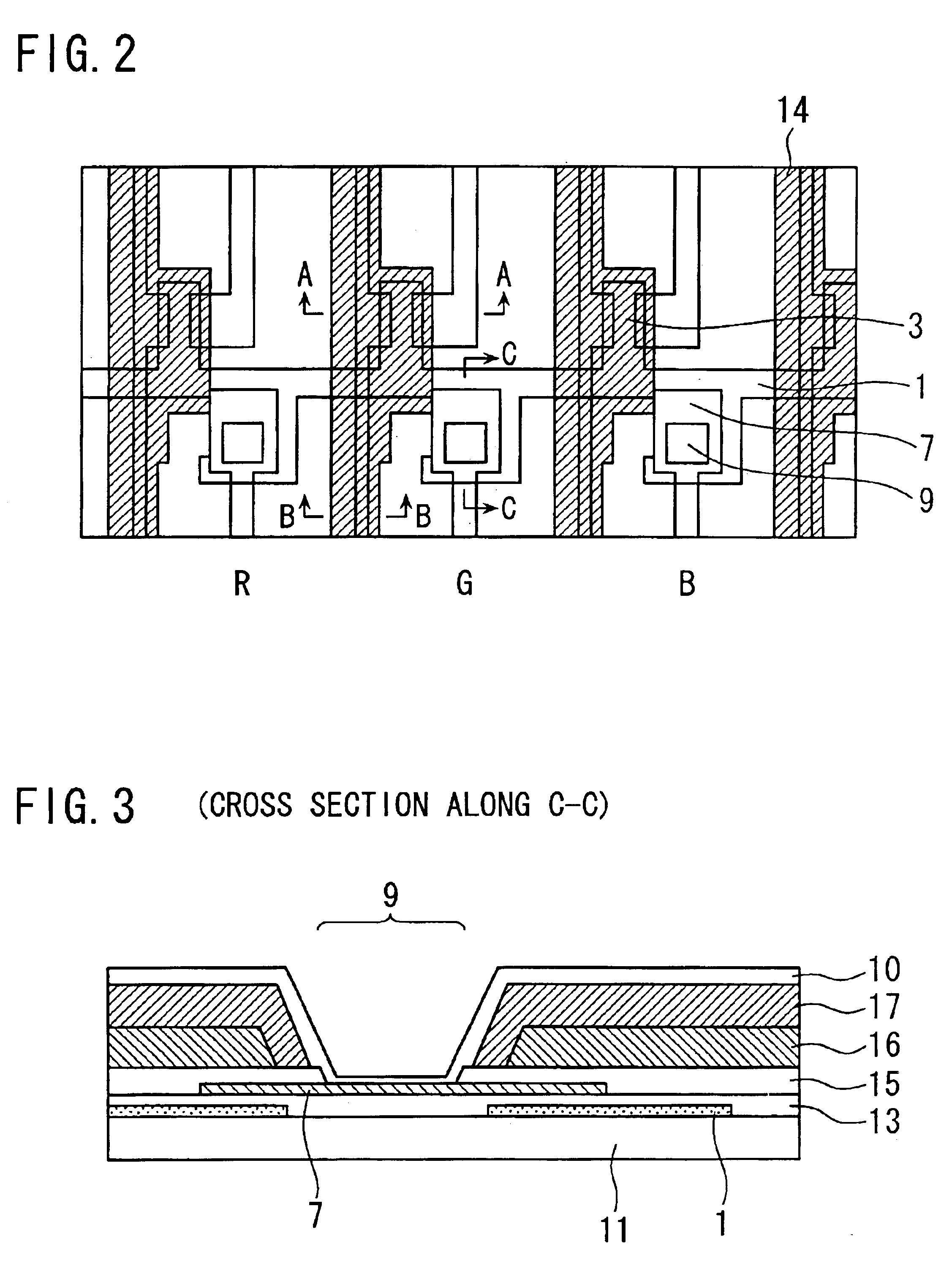
In a conventional liquid crystal display in which a color filter and a light shield film are disposed on the side of an opposing substrate, it was difficult to maximize an area of an aperture portion of each pixel, that is, it was difficult to maximize an aperture ratio of each pixel.
This is because, in such liquid crystal display, since there is a possibility that an error occurs in the alignment of pixel locations between a TFT substrate and an opposing substrate in a fabrication process in which the TFT substrate and the opposing substrate are assembled.
Even when the passivation film is removed thereafter, it is impossible to remove the portion of the passivation film just under the light shield film resin remained after development.
Therefore, contact of the drain electrode or the drain signal line with the pixel electrode is deteriorated, and such deterioration of contact causes a dot defect.
In this way, when the light shield film is formed in a grid shape or a matrix, there is high possibility that defective contacts, i.e., dot defects are caused by the residue of the light shield film resin after development.

Method used


Image

  • CF on TFT liquid crystal display having reduced dot defects
  • CF on TFT liquid crystal display having reduced dot defects
  • CF on TFT liquid crystal display having reduced dot defects

Examples


second embodiment

Next, with reference to the drawings, an explanation will be made on the present invention.

FIG. 9 is a schematic plan view of liquid crystal display panels which are formed on a glass substrate and which are under fabrication. FIG. 9 also includes an enlarged partial view of one of the liquid crystal display panels formed on the glass substrate. For example, assume that liquid crystal display panels 72 each having a size of 6.3 inches are to be disposed effectively on a glass substrate 71 having the sizes of 370 mm×470 mm. In such case, as shown in FIG. 9, it is possible to dispose, on the glass substrate 71, four panels 72 along the longitudinal direction of the glass substrate 71 and two panels 72 along the direction perpendicular to the longitudinal direction of the glass substrate 71. Therefore, a total of eight liquid crystal display panels 72 are formed on the glass substrate 71. Also, as can be seen from the partial enlarged view of the liquid crystal display panel 72, each o...


PUM


Abstract

A CF on TFT type liquid crystal display and a method of manufacturing the same. The liquid crystal display has a plurality of parallel scanning lines, a plurality of parallel data lines which cross the scanning lines, thin film transistors each disposed in the proximity of an intersection between one of the scanning lines and one of the data lines, and pixel electrodes disposed in a matrix and each coupled with one of the thin film transistors. The light shield film is formed over areas including at least the thin film transistors but except over portions which become banks and hinder flow of developer for patterning the light shield film. As an embodiment, the light shield film can be formed along the data lines, and also partially along the scanning lines except a part of each portion of the scanning lines between adjacent data lines.

Description

FIELD OF THE INVENTIONThe present invention relates generally to a liquid crystal display and a method of manufacturing the same. More particularly, the present invention relates to a liquid crystal display which has a CF on TFT (color filter on thin film transistor) structure and which has reduced dot defects.BACKGROUND OF THE INVENTIONIn order to realize a liquid crystal display having high resolution, it is necessary to increase a density of disposition of pixels. In a conventional liquid crystal display in which a color filter and a light shield film are disposed on the side of an opposing substrate, it was difficult to maximize an area of an aperture portion of each pixel, that is, it was difficult to maximize an aperture ratio of each pixel. This is because, in such liquid crystal display, since there is a possibility that an error occurs in the alignment of pixel locations between a TFT substrate and an opposing substrate in a fabrication process in which the TFT substrate an...

Claims


Application Information

Patent Timeline
IPC IPC(8): G02F1/13G02F1/1362G02F1/1335G02F1/136G02F1/1368
CPCG02F1/136209G02F1/136227G02F1/136
Inventor OKAMOTO, MAMORUSAKAMOTO, MICHIAKIHIDEHIRA, MASANOBU
Owner VISTA PEAK VENTURES LLC
Why Eureka
Try Eureka