Semiconductor stress sensor

Active Publication Date: 2021-06-10
MELEXIS TECH NV
View PDF3 Cites 1 Cited by
  • Summary
  • Abstract
  • Description
  • Claims
  • Application Information

AI Technical Summary

Benefits of technology

The present invention provides a piezo-resistor sensor with several technical advantages. First, it prevents leakage currents between neighboring piezo-diffusion regions caused by inversion of the bulk between them. Second, it reduces modulation caused by a charge above a well region next to a piezo-diffusion region that creates enough inversion at the well surface to provide a leakage from one point of the diffusion path with higher voltage to another point of the diffusion path with lower voltage or even to another diffusion path of another resistor. Third, it can make use of the same material for its conductive shield and interconnect structures, which simplifies the manufacturing process. Finally, it reduces modulation of the piezo-diffusion by adding highly doped islands that are covered by the conductive interconnect structure on one side and by the conductive shield on another side.

Problems solved by technology

This solution has, however, as drawback that a second metallic shield layer has to be placed over the interconnect to cover it.
This involves extra processing effort.
Another disadvantage is that the piezo resistors get further away from the surface leading to a significant loss of sensitivity.
Therefore this solution will fail for very high charging of the surface.
Another issue is that the gap between the shield and highly doped p-diffusions still can provide a path for leakage currents to other structures.
In that case, however, metal is disposed over the membrane which will lead to drift due to plastic deformation of this metal and again inversion can take place between the metal lines which still provide a path for leaking from one resistor to another resistor.

Method used


Image

  • Semiconductor stress sensor
  • Semiconductor stress sensor
  • Semiconductor stress sensor

Examples


Embodiment Construction

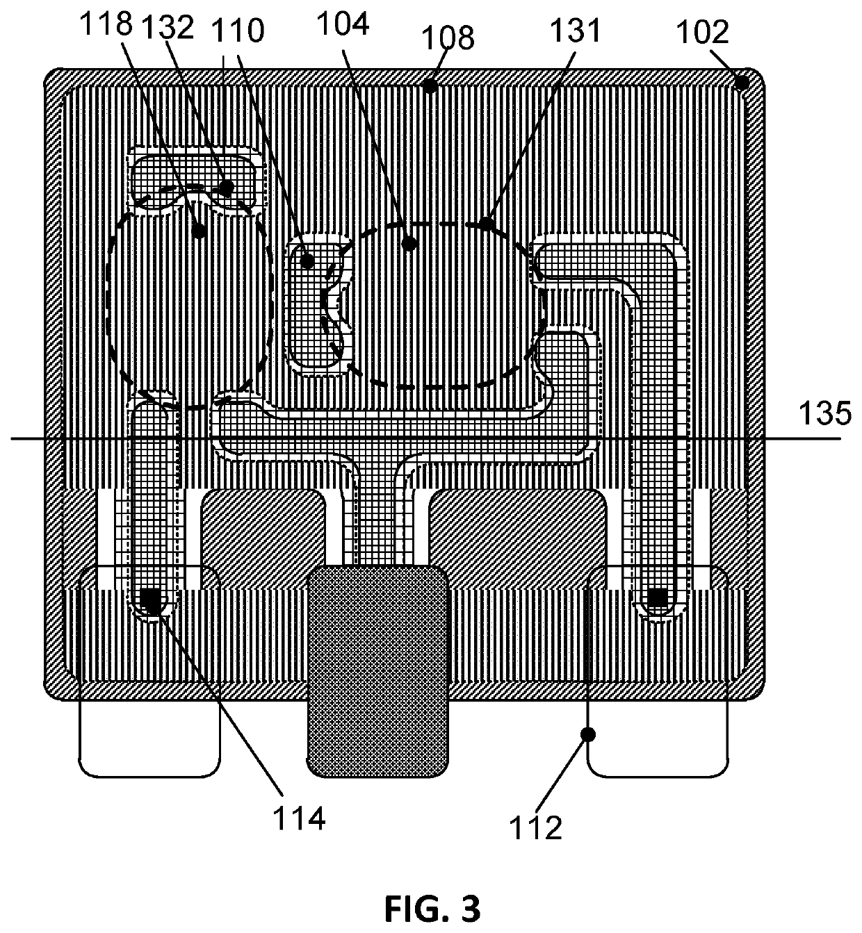
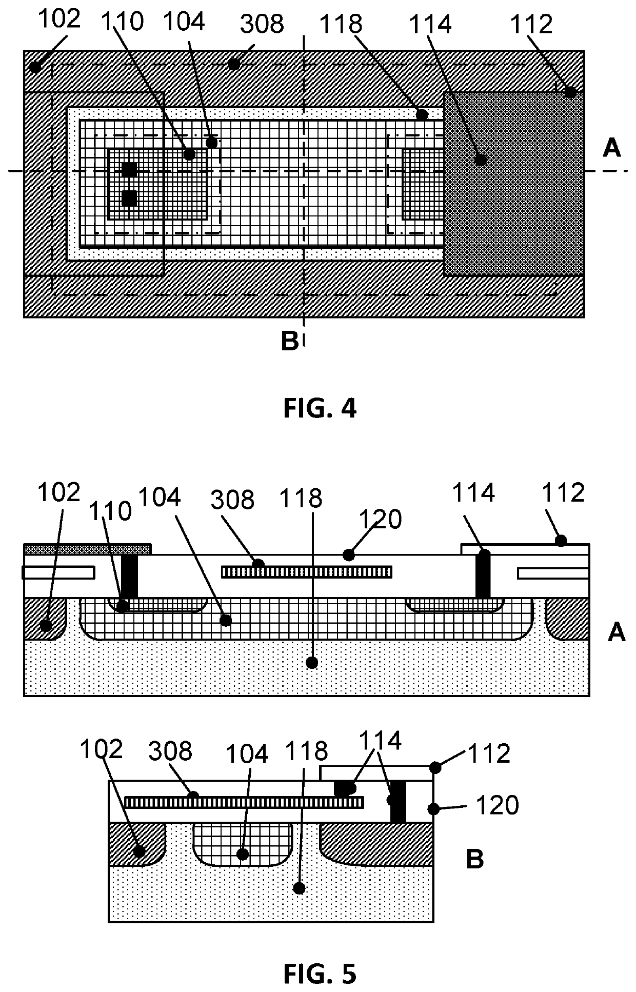
[0066]The present invention will be described with respect to particular embodiments and with reference to certain drawings but the invention is not limited thereto but only by the claims. The drawings described are only schematic and are non-limiting. In the drawings, the size of some of the elements may be exaggerated and not drawn on scale for illustrative purposes. The dimensions and the relative dimensions do not correspond to actual reductions to practice of the invention.

[0067]It is to be noticed that the term “comprising”, used in the claims, should not be interpreted as being restricted to the means listed thereafter; it does not exclude other elements or steps. It is thus to be interpreted as specifying the presence of the stated features, integers, steps or components as referred to, but does not preclude the presence or addition of one or more other features, integers, steps or components, or groups thereof. Thus, the scope of the expression “a device comprising means A ...


PUM


Abstract

A piezo-resistor sensor includes a diffusion of a first conductivity type in a well of an opposite second type, contacts with islands in the diffusion, interconnects with the contacts, and a shield covers the diffusion between the contacts and extends over side walls of the diffusion between the contacts. Each interconnect covers the diffusion at the corresponding contact and extends over edges of the diffusion, and each island is at a side covered by its interconnect. A guard ring of the second type is around the diffusion. The shield covers the well between the diffusion and the ring and the edge of the ring facing the diffusion. If a gap between the shield and the interconnect is present, the ring bridges this gap, and / or the edges of the diffusion are completely covered by the combination of the shield and the interconnects.

Description

FIELD OF THE INVENTION[0001]The invention relates to the field of semiconductor stress sensing elements. More specifically it relates to piezo-resistor based stress sensors.BACKGROUND OF THE INVENTION[0002]A semiconductor stress sensing element comprises a diffusion path of a first conductivity type defined in a lowly doped well of a second, opposite conductivity type. The sections of the diffusion path that have to be stress sensitive are lowly doped and other sections that should not be stress sensitive are highly doped or even consist of a metal-silicon alloy. The sheet resistance of the diffusion path is inversely proportional on the level of doping. The sheet resistance of a lowly doped diffusion path is typically between 300 and 5000 ohm / square, whereas the sheet resistance of a high doped area is typically between 20 and 150 ohm / square. When an alloy is formed at the surface of a highly doped area, the sheet resistance even drops to only 1 to 5 ohm / square. Typically highly do...

Claims


Application Information

Patent Timeline
IPC IPC(8): H01L41/113H01L41/047H01L41/053G01L1/18
CPCH01L41/1132G01L1/18H01L41/053H01L41/0475H01L23/552G01L1/2293H10N30/302H10N30/88H10N30/875
Inventor VAN DER WIEL, APPOLONIUS JACOBUSRAMEZANI, MALIHEHROOMAN, CATHLEENOTTE, LAURENTVERGAUWEN, JOHAN
Owner MELEXIS TECH NV
Why Eureka
Try Eureka