Circuits employing on-diffusion (OD) edge (ODE) dummy gate structures in cell circuit with increased gate dielectric thickness to reduce leakage current

a dummy gate and cell circuit technology, applied in the field of transistors, can solve the problems of increasing current leakage, reducing the isolation between the dummy gate structure and the active semiconductor structure, and increasing current leakage, so as to increase the volume of work function, reduce leakage current, and increase the dielectric thickness of the ga

Inactive Publication Date: 2021-04-22
QUALCOMM INC
View PDF0 Cites 0 Cited by
  • Summary
  • Abstract
  • Description
  • Claims
  • Application Information

AI Technical Summary

Benefits of technology

[0005]Aspects disclosed herein include circuits employing on-diffusion (OD) edge (ODE) dummy gate structures in cell circuit with increased gate dielectric thickness to reduce leakage current. An integrated circuit (“circuit”) is provided that includes at least one active semiconductor region (also referred to as “diffusion region”) formed in a substrate. For example, the circuit can include a P-type active semiconductor region(s) and an N-type active semiconductor region(s) (e.g. diffusion regions) formed in a substrate to form complementary metal oxide semiconductor (CMOS) circuits. A diffusion barrier can be formed on an edge of the circuit to provide isolation between a cell circuit and an adjacent cell circuit formed on the substrate. One or more active semiconductor structures (e.g., a fin) of the cell circuit are formed in the active semiconductor regions to form semiconductor channels for field effect transistors (FETs). A plurality of gates are formed over the active semiconductor structures to provide gates for FETs and / or routing in a cell circuit. One or more of the gates are dummy gates that are ODE dummy gate structures formed over ends of the active semiconductor structure(s) at the edge of the cell circuit to provide an additional dummy gate pattern to protect an active gate during the fabrication of the circuit. Because the ODE dummy gate structures are disposed over ends of the active semiconductor structure, gaps may be present that are adjacent to the ends of the active semiconductor structures, allowing for an increased volume of work function metal structures to be formed for the ODE dummy gate structures and thus leading to leakage current. Opening and etching the ODE dummy gate structure area of the cell circuit when forming dummy gates in the cell circuit can cause the gate dielectric structure disposed on the active semiconductor structure to be damaged, thus reducing isolation between an ODE dummy gate structure and the active semiconductor structure. A reduced isolation between the ODE dummy gate structure and the active semiconductor structure can increase current leakage.

Problems solved by technology

Because the ODE dummy gate structures are disposed over ends of the active semiconductor structure, gaps may be present that are adjacent to the ends of the active semiconductor structures, allowing for an increased volume of work function metal structures to be formed for the ODE dummy gate structures and thus leading to leakage current.
Opening and etching the ODE dummy gate structure area of the cell circuit when forming dummy gates in the cell circuit can cause the gate dielectric structure disposed on the active semiconductor structure to be damaged, thus reducing isolation between an ODE dummy gate structure and the active semiconductor structure.
A reduced isolation between the ODE dummy gate structure and the active semiconductor structure can increase current leakage.

Method used


Image

  • Circuits employing on-diffusion (OD) edge (ODE) dummy gate structures in cell circuit with increased gate dielectric thickness to reduce leakage current
  • Circuits employing on-diffusion (OD) edge (ODE) dummy gate structures in cell circuit with increased gate dielectric thickness to reduce leakage current
  • Circuits employing on-diffusion (OD) edge (ODE) dummy gate structures in cell circuit with increased gate dielectric thickness to reduce leakage current

Examples


Embodiment Construction

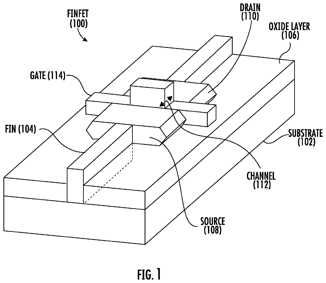
[0024]With reference now to the drawing figures, several exemplary aspects of the present disclosure are described. The word “exemplary” is used herein to mean “serving as an example, instance, or illustration.” Any aspect described herein as “exemplary” is not necessarily to be construed as preferred or advantageous over other aspects.

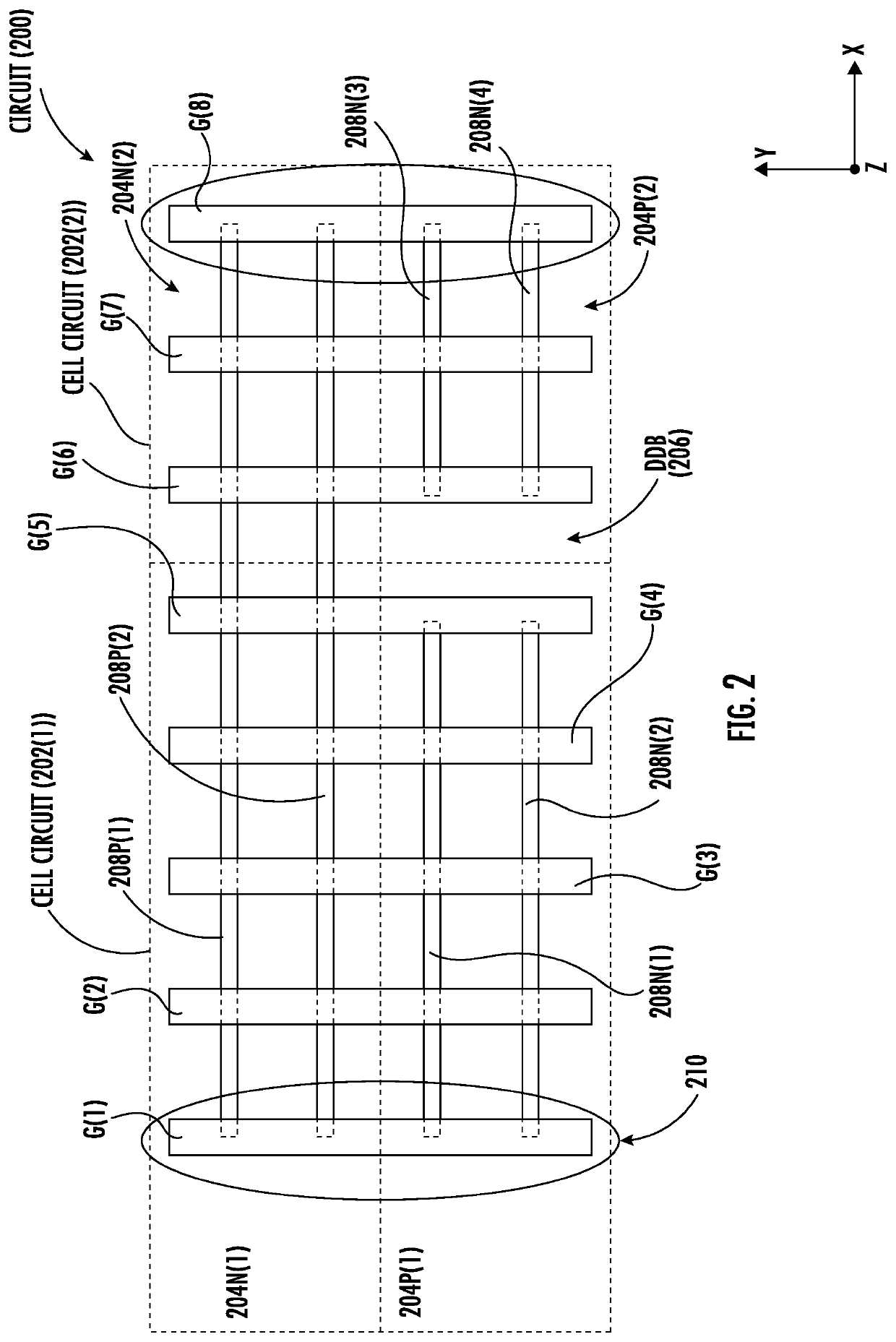
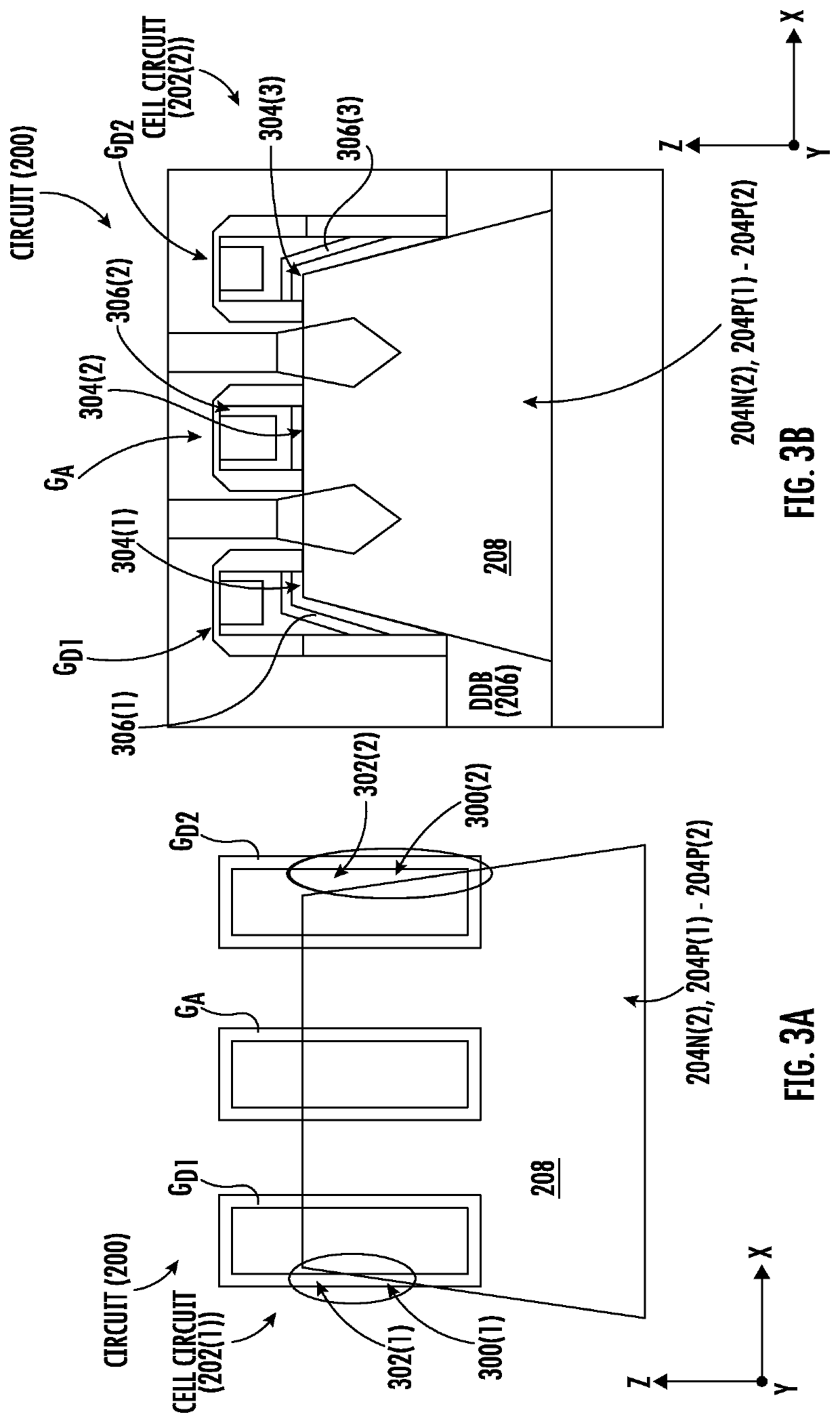
[0025]Aspects disclosed herein include circuits employing on-diffusion (OD) edge (ODE) dummy gate structures in cell circuit with increased gate dielectric thickness to reduce leakage current. An integrated circuit (“circuit”) is provided that includes at least one active semiconductor region (also referred to as “diffusion region”) formed in a substrate. For example, the circuit can include a P-type active semiconductor region(s) and an N-type active semiconductor region(s) (e.g. diffusion regions) formed in a substrate to form complementary metal oxide semiconductor (CMOS) circuits. A diffusion barrier can be formed on an edge of the circuit to prov...


PUM

PropertyMeasurementUnit
semiconductoraaaaaaaaaa
thicknessaaaaaaaaaa
work functionaaaaaaaaaa

Abstract

Circuits employing on-diffusion (OD) edge (ODE) dummy gate structures in cell circuit with increased gate dielectric thickness to reduce leakage current are disclosed. A gate dielectric structure may be formed between a work function metal structure of an ODE dummy gate structure and an active semiconductor structure in a cell circuit, and is provided to be thicker than a gate dielectric structure formed between a work function metal structure and an active gate(s) in the cell circuit. Providing a gate dielectric structure of increased thickness can reduce damage to the gate dielectric structure providing isolation between the ODE dummy gate structure and the active semiconductor structure. Providing a gate dielectric structure of increased thickness can also reduce the gap area adjacent to the ends of the active semiconductor structures and thus reduce the volume of work function metal structure formed in the gaps to further reduce leakage current.

Description

PRIORITY[0001]The present application claims priority under 35 U.S.C. § 119(e) to U.S. Provisional Patent Application Ser. No. 62 / 923,385, filed on Oct. 18, 2019 and entitled “CIRCUITS EMPLOYING ON-DIFFUSION (OD) EDGE (ODE) DUMMY GATE STRUCTURES IN CELL CIRCUIT WITH THICKER GATE DIELECTRIC TO REDUCE LEAKAGE CURRENT,” the contents of which is incorporated herein by reference in its entirety.BACKGROUNDI. Field of the Disclosure[0002]The field of the disclosure relates to transistors, such as Fin Field-Effect Transistors (FETs) (FinFETs) in integrated circuits (ICs), and more particularly to use of on-diffusion (OD) edge (ODE) dummy gate structures (e.g., poly (metal gate) OD edge (PODE) structures) on cell circuit edges to protect ends of semiconductor fins of FETs.II. BACKGROUND[0003]Transistors are essential components in modern electronic devices. Large numbers of transistors are employed in integrated circuits (ICs) in many modern electronic devices. For example, components such a...

Claims


Application Information

Patent Timeline
Patent Type & Authority Applications(United States)
IPC IPC(8): H01L29/06H01L27/088H01L21/8234
CPCH01L29/0607H01L21/823431H01L21/823437H01L27/0886H01L21/823481
Inventor LI, XIAYANG, HAININGYANG, BIN
Owner QUALCOMM INC
Why Eureka
Try Eureka