Method for depositing silicon oxide film having improved quality by peald using bis(diethylamino)silane
a technology of silicon oxide film and bis(diethylamino)silane, which is applied in the direction of coating, chemical vapor deposition coating, metallic material coating process, etc., can solve the problems that the duration of an rf power pulse may not be sufficient or effective to improve film quality, and the increase of rf power and/or pulse duration may not be sufficient. to achieve the effect of suppressing the thermal decomposition of bdeas and significantly improving the quality of the deposited film
- Summary
- Abstract
- Description
- Claims
- Application Information
AI Technical Summary
Benefits of technology
Problems solved by technology
Method used
Image
Examples
reference example 1 (
Thermal Stability of BDEAS)
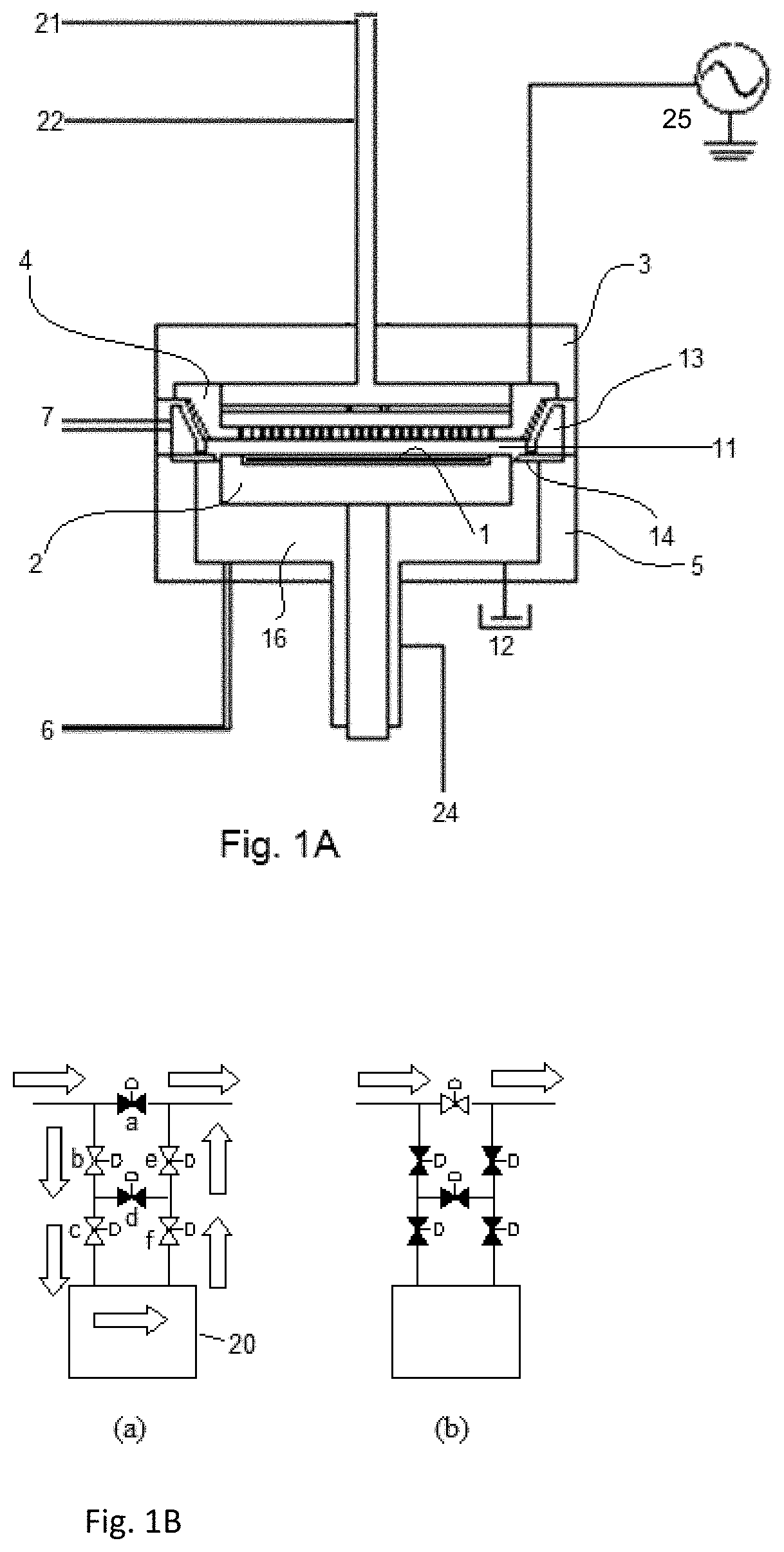
[0038]In Reference Example 1, in order to examine thermal stability of BDEAS, a Si substrate on which a native or natural oxide film having a thickness of 1.20 nm was formed was placed in the apparatus illustrated in FIG. 1A with a gas supply system (FPS) illustrated in FIG. 1B. The atmosphere of the reaction chamber was controlled by feeding thereto BDEAS at 2000 sccm and oxygen at 2000 sccm under a pressure of 400 Pa without applying RF power to the reaction chamber, wherein a susceptor temperature was set in a range of 400° C. to 650° C. 800 seconds after the susceptor temperature reached the set temperature, the thickness of the film was measured at each set temperature. As a comparative reference example, the thickness of film was measured at each set temperature in the same manner as in Reference Example 1 except that no BDEAS was fed to the reaction chamber.
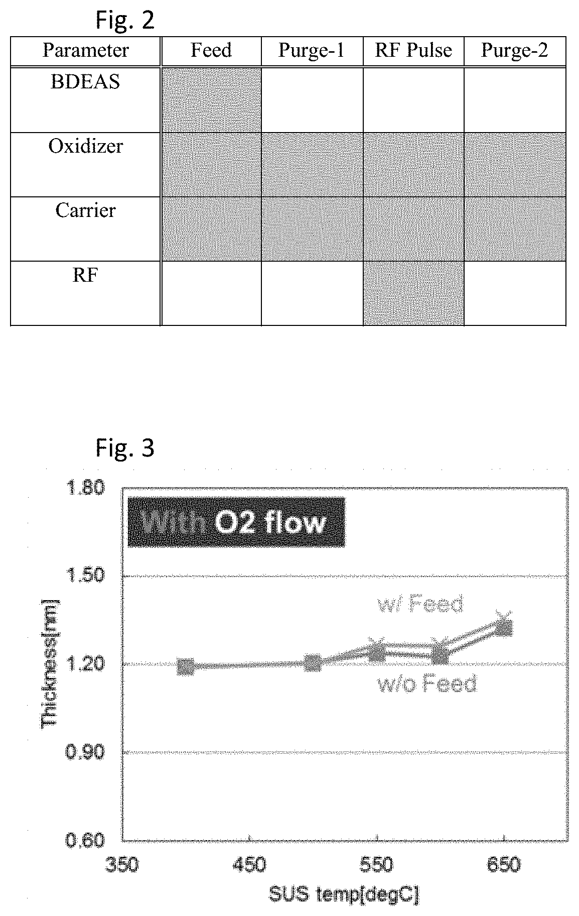
[0039]FIG. 3 shows a graph indicating the schematic relationship between film thickness and s...
example 1 (
Improvement of Film Quality at High Deposition Temperatures)
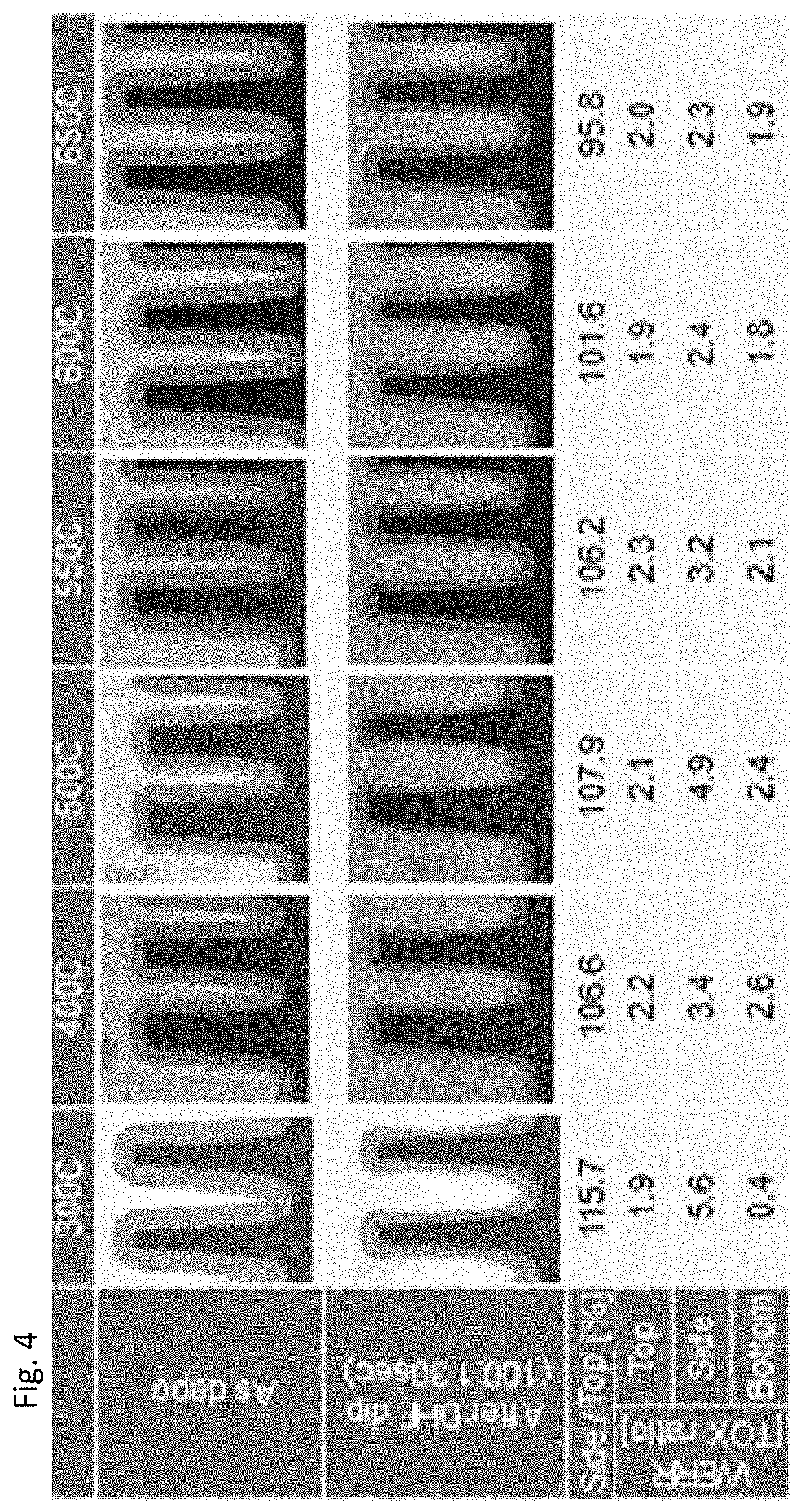
[0040]A silicon oxide film was deposited on a Si substrate (having a diameter of 300 mm and a thickness of 0.7 mm) having trenches with an opening of approximately 30 nm, which had a depth of approximately 90 nm (an aspect ratio was approximately 3), by PEALD process in order to determine film quality of the film, under the conditions shown in Table 1 below (varying the deposition temperature) in the process sequence illustrated in FIG. 2 using the apparatus illustrated in FIG. 1A and a gas supply system (FPS) illustrated in FIG. 1B. After deposition of silicon oxide film was complete, a cross-sectional view of each substrate with the trenches was photographed using STEM.
TABLE 1(numbers are approximate)Temp. settingSUS temp (° C.).See FIG. 4DepoPressure (Pa)400Electrode Gap (mm)7.5Feed time (s)0.2Purge-1 (s)0.3RF time (s)1Purge-2 (s)0.1RF power (W)500PrecursorBDEASCarrierArCarrier flow (slm)2.0Dilution Ar (slm)2.0Seal He (s...
example 2 (
Improvement of Film Quality with Other Parameters)
[0043]A silicon oxide film was deposited on a Si substrate in the same manner as in Example 1 except the conditions shown in Table 2 below.
TABLE 2(numbers are approximate)Temp.UHT-6UHT-7UHT-8UHT-9UHT-10UHT-11settingSUS temp (° C.).650DepoPressure (Pa)40040010003000400400Purge-1 (s)0.32220.30.3Carrier Ar (slm)2.02.02.02.02.00.4Dilution Ar (slm)2.02.02.02.05.62.0O2 (slm)4.04.04.04.00.45.6O2 / (O2 + Ar) (%)50505050570
[0044]After completion of deposition of each silicon oxide film, the substrate was subjected to wet etching in the same manner as in Example 1. Further, after wet etching, a cross-sectional view of each substrate with the trenches was photographed using STEM. It should be noted that when the deposition pressure was 3,000 Pa in UHT-9, film deposition became highly abnormal and thus, wet etch evaluation of this sample was not conducted.
[0045]FIG. 5 is a chart showing STEM photographs of cross-sectional views of the trenches sub...
PUM
| Property | Measurement | Unit |
|---|---|---|
| temperature | aaaaa | aaaaa |
| temperature | aaaaa | aaaaa |
| pressure | aaaaa | aaaaa |
Abstract
Description
Claims
Application Information
 - R&D
- Intellectual Property
- Life Sciences
- Materials
- Tech Scout
- Unparalleled Data Quality
- Higher Quality Content
- 60% Fewer Hallucinations
Browse by: Latest US Patents, China's latest patents, Technical Efficacy Thesaurus, Application Domain, Technology Topic, Popular Technical Reports.
© 2025 PatSnap. All rights reserved.Legal|Privacy policy|Modern Slavery Act Transparency Statement|Sitemap|About US| Contact US: help@patsnap.com


