
Wave propagation computing devices for machine learning

a computing device and wave propagation technology, applied in computing models, biological models, instruments, etc., can solve the problems of prohibitive resources, and high cost of computer hardware and software, etc., to process large and sparse data sets

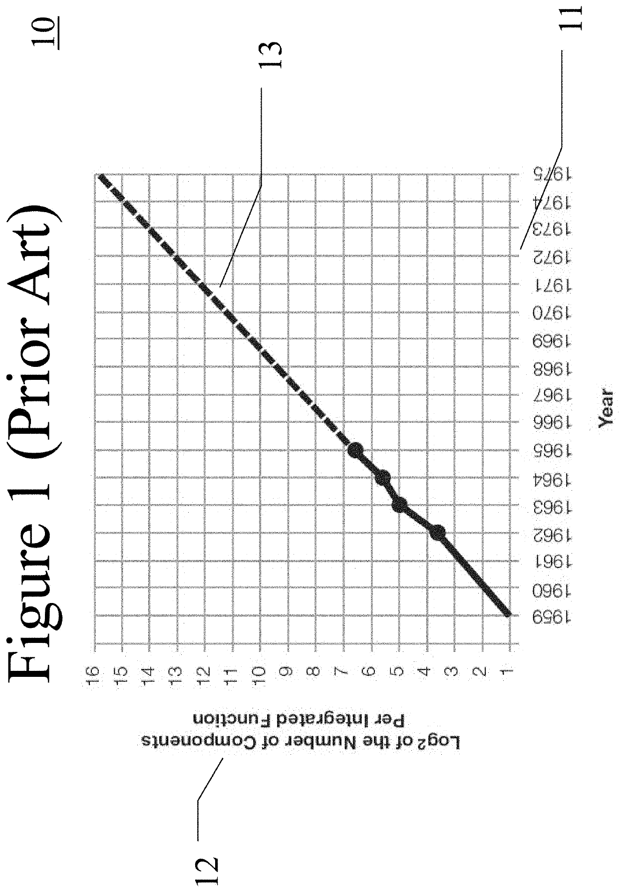
Inactive Publication Date: 2020-04-30
CYMATICS LAB CORP
View PDF0 Cites 4 Cited by
  • Summary
  • Abstract
  • Description
  • Claims
  • Application Information

AI Technical Summary

Benefits of technology

The present technology describes an acoustic-wave reservoir computing (AWRC) device that uses random projections to perform computations. The device takes in multiple electrical input signals and delivers multiple output signals. It uses an analog random projection medium that has asymmetric geometrical boundaries and provides non-linear propagation of signal waves. The device includes a suspension structure that isolates the cavity from the environment. The method involves sending electrical input signals to input transducers, physically propagating the signal waves in the medium, and receiving output signals from output transducers. The output signals can be processed for signal processing and machine learning. The device has potential applications in machine learning and signal processing.

Problems solved by technology

Today, much of the recorded data consists of images and videos, which both possesses attributes (or features) that number from the thousands to the millions, and both are typically extremely sparse.
Traditional statistical analysis techniques were developed for smaller and denser data sets, and require prohibitive resources (in cost of computer hardware, and cost of electrical power) to process large and sparse data sets.
As a result, the cost and speed of new computer chips is expected to level off within 10 years, and the computer revolution risks slowing down or stopping altogether.
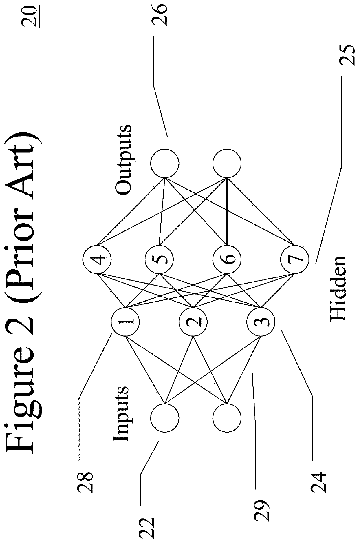
But, neural network computational techniques are resource-intensive; even a moderately-complex neural network architecture requires significant computational resources—CPU time, memory and storage.
However, GPUs consume 100's of watts of power, and must be placed on cooled racks, and are therefore not suitable for portable applications.
However, to achieve high performance, digital circuit implementations of neural networks require the use of the most advanced, and therefore the most expensive, semiconductor circuit manufacturing technologies available to-date, which result in a high per-unit cost of digital neural networks.
However, with every new generation of CMOS technology below 65 nm, analog circuits lose some of their performance advantage over digital circuits: the voltage gain of MOSFETs keeps decreasing, and the performance variability between MOSFETS that are designed to be identical keeps increasing.
Both of these basic trends make analog circuits larger and more complex (to make up for the poor voltage gain or / and to correct transistor-to-transistor variability issues), which directly increases the size and power consumption of analog circuits, and thus decreases their performance advantage over digital circuits.
As a result, analog circuit implementations of neural networks offer only a limited cost and power improvement over digital circuit neural networks, and alternate fabrication methods or / and computing schemes are needed.
However, to-date, optics-based implementations of neural network computation circuits are bulky and costly (compared to all-semiconductor implementations) due to the lack of very-small-size low-cost light modulation circuits (which are required to generate signals and perform multiplications), and it is not yet apparent how this basic technological may get resolved.
As stated above, many types of very large data sets are very sparse in their attribute or feature space.
This occurs because it is nearly impossible to obtain a uniform sampling of points along every attribute / feature axis.
As a result, in the high-dimensional feature space (generally a Hilbert space), the vectors of very large data sets are distributed very sparsely.
Random projection is traditionally implemented on general-purpose computers, and so suffers from the limitations of common CPU systems: comparatively high power consumption, and a limited speed due to the CPU / DRAM memory bottleneck.
Such a system would have a high data throughput, but the proposed implementation is large and comparatively costly.
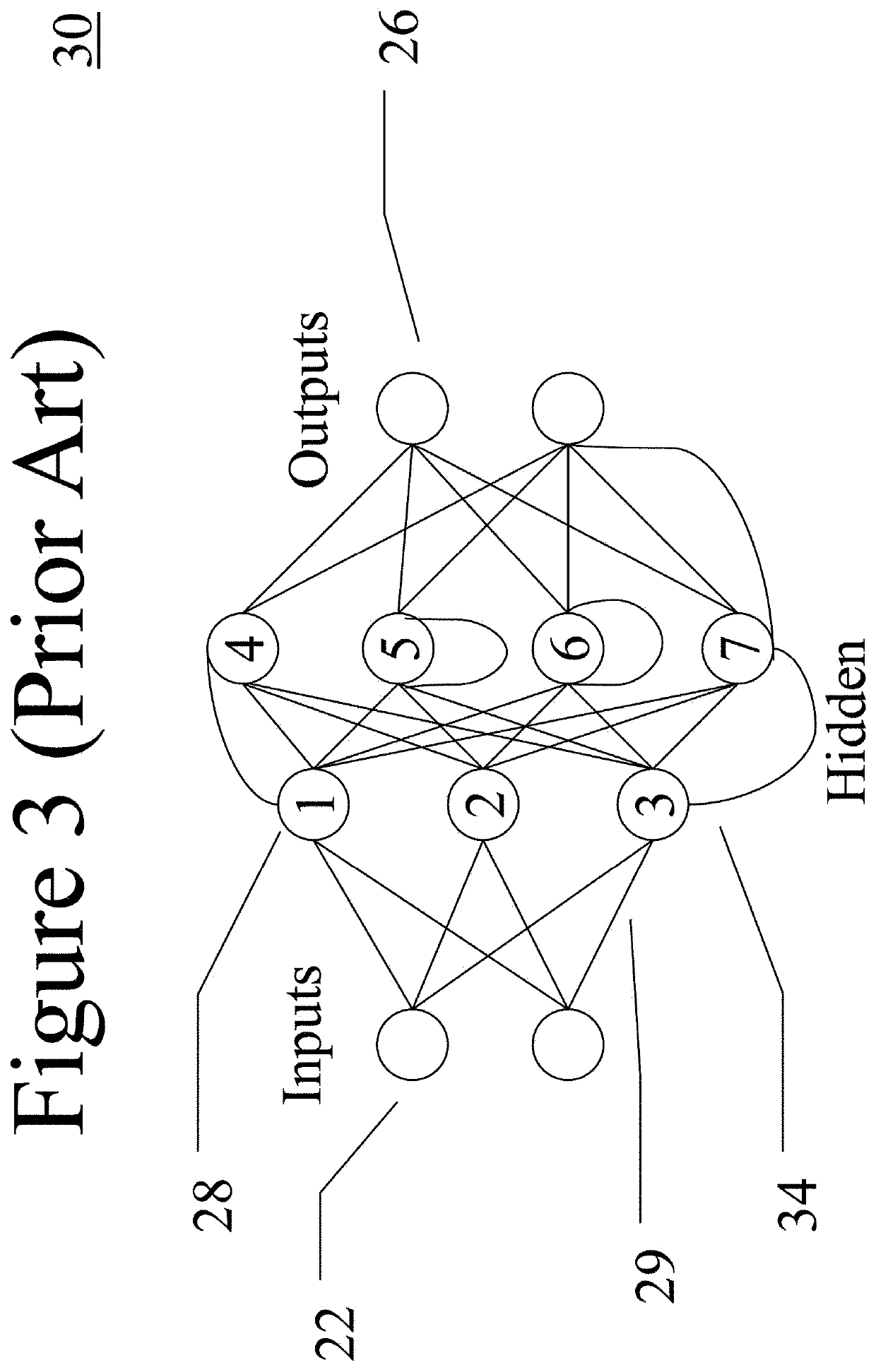
However, when used for classification applications, this type of implementation involves a massive amount of computations (the state of every neuron in the reservoir must be explicitly computed at every time step) even though a small number of those computations is required to perform the classification task.
As a result, digital electronic implementations of reservoir computing networks have comparatively high power consumption.
Reservoir computing networks have also been implemented using optical techniques, but many such demonstrations use an optical fiber as reservoir (i.e. the reservoir of randomly- and recurrently-connected neurons is replaced by a simple delay line), which reduces the functionality and computational capability of these networks.
Other optics-based demonstrations use optical components that are comparatively large and costly.
Finally, reservoir computing networks have been implemented using water as reservoir, but such demonstrations do not scale beyond limited proof-of-concept examples.

Method used


Image

  • Wave propagation computing devices for machine learning
  • Wave propagation computing devices for machine learning
  • Wave propagation computing devices for machine learning

Examples


embodiment 120

[0188]FIG. 15 is a diagram that depicts a finite-element solid model 150 of an alternate embodiment of a reservoir that is similar to embodiment 120 of FIG. 12, seen at an angle from the top. The model is drawn to scale in the plane, but layer thicknesses are exaggerated for clarity. The cavity 121 has an asymmetric geometry as well as internal boundaries 122, in the form of through-holes. The cavity is surrounded by piezoelectric TE-mode transducer material layer 124, though LE-mode or SAW transducers can also be manufactured. Passive or active temperature compensation of the transducer response is optionally included. A top conductive electrode 123 defines the electro-mechanically active region of each transducer. A lower conductive electrode 128 is present under at least the transducer material layer 124. Electrode 128 may also be present under the cavity 121. Transducers 127 are used for input and output and may optionally be used for feedback, self-test or remain unused.

[0189]F...

embodiment 190

[0193]FIG. 20 is a diagram that depicts a cross-section 200 of embodiment 190 presented on FIG. 19. The lower conductive electrode is the layer 141. The cavity material is the layer 142. Layer 142 can be a linear, non-linear, piezoelectric, electrostrictive or photoelastic material or stack of materials. This layer contains patterned holes or inclusions that may go through the entire thickness of the layer 145, or partial through the thickness of the layer 146. The TE-or LE-mode transducer 204 is placed on top of the cavity 142. It consists of conductive top and bottom electrode 144, a piezoelectric layer 143. The piezoelectric layer 143 can additionally have electrostrictive or photoelastic properties. The conductive electrode layers 144 are on top and bottom of the piezoelectric layer 143. They form the electrical ports 147 to which the AWRC device is connected to other circuits. Acoustic coupler 202 can optionally be used to decouple the electrical response of the transducer 204 ...


PUM


Abstract

Embodiments of the present technology may be directed to wave propagation computing (WPC) device(s), such as an acoustic wave reservoir computing (AWRC) device, that performs computations by random projection. In some embodiments, the AWRC device is used as part of a machine learning system or as part of a more generic signal analysis system. The AWRC device takes in multiple electrical input signals and delivers multiple output signals. It performs computations on these input signals to generate the output signals. It performs the computations using acoustic (or electro-mechanical) components and techniques, rather than using electronic components (such as CMOS logic gates or MOSFET transistors) as is commonly done in digital reservoirs.

Description

CROSS-REFERENCE TO RELATED APPLICATION[0001]The present application claims the benefit of the filing date of U.S. Provisional Application No. 62 / 520,167 filed Jun. 15, 2017, the disclosure of which is hereby incorporated herein by reference.TECHNICAL FIELD[0002]The present technology concerns a wave propagation computing (WPC) device, such as an acoustic wave reservoir computing (AWRC) device, for performing computations by random projection. In some applications, the AWRC device may be used for signal analysis or machine learning.BACKGROUND[0003]The field of computer and information technology is being impacted simultaneously by two fundamental changes: (1) the types and quantity of data being collected is growing exponentially; and (2) the increase in raw computing power over time (i.e. Moore's Law) is slowing down and may stop altogether within 10 years.[0004]It is estimated that human activity generates 2.5 quintillion (2.5×10¹⁸) bytes of data per day. Up to the recent past, rec...

Claims


Application Information

Patent Timeline
Patent Type & Authority Applications(United States)
IPC IPC(8): B81B3/00H01L41/09H01L27/20G06N3/04H10N30/00H10N30/20H10N30/85H10N39/00
CPCG06N3/04H01L41/0986B81B3/0021H01L27/20G06N3/065G06N3/044H10N30/206H03H9/02015H03H9/02244H03H9/0296H10N39/00
Inventor SINHA, RAJARISHIGUILLOU, DAVID FRANCOIS
Owner CYMATICS LAB CORP
Learn More