Multi-wafer bonding structure and bonding method

a multi-wafer bonding and bonding technology, applied in the direction of semiconductor devices, semiconductor/solid-state device details, electrical devices, etc., can solve the problems of slow signal transmission, large signal delay and power loss, unfavorable increase of integration density, etc., to achieve short interconnection distance, low power consumption, and high signal transmission rate

Active Publication Date: 2020-03-05
WUHAN XINXIN SEMICON MFG CO LTD
View PDF2 Cites 1 Cited by
  • Summary
  • Abstract
  • Description
  • Claims
  • Application Information

AI Technical Summary

Benefits of technology

[0015]The present invention provides a multi-wafer bonding structure and bonding method. The multi-wafer bonding structure comprises a first unit and a second unit. The first unit comprises an upper wafer of the first unit and a lower wafer of the first unit that are bonded to each other. The second unit comprises at least one wafer. The upper wafer of the first unit and the second unit are bonded to each other. A metal layer of each wafer in the first unit is electrically connected to an interconnection layer of the first unit. A first bonding layer in the first unit is electrically connected to the interconnection layer of the first unit. A second bonding layer in the second unit is electrically connected to a metal layer of the second unit. The first bonding layer is in contact with the second bonding layer so as to achieve an electrical connection, thereby achieving the electrical connection among the interconnection layer of the first unit, the first bonding layer, the second bonding layer and the metal layer of each wafer, which does not need an external lead wire structure, since the interconnection structure of the whole multi-wafer bonding structure is arranged inside the wafer. Compared to the prior art, the multi-wafer bonding structure of the present invention has the advantages of a short interconnection distance, a high signal transmission rate and a low power consumption, and is favorable for achieving a high-density multi-wafer integration and a multifunctional wafer integration.
[0016]In addition, the first trench and the lead-out layer are formed. The lead-out layer is formed at the bottom of the first trench and electrically connected to the metal layer of the topmost wafer. Compared to the conventional technique, the formation of the lead-out layer at the bottom of the first trench eliminates the process of firstly filling the whole trench with a metal layer (e.g., copper) and then processing the filling metal layer (e.g., copper) in the lead-out layer, thereby being favorable for reducing the cost.

Problems solved by technology

However, the lead wire bonding of the chip stacking and the solder ball soldering of the package-on-package have the defects of long interconnection distance, slow signal transmission, large signal delay and large power loss.
Besides, the lead wires and the solder balls also occupy a large packaging space, which is not conducive to the increase of the integration density.

Method used


Image

  • Multi-wafer bonding structure and bonding method
  • Multi-wafer bonding structure and bonding method
  • Multi-wafer bonding structure and bonding method

Examples


embodiment 1

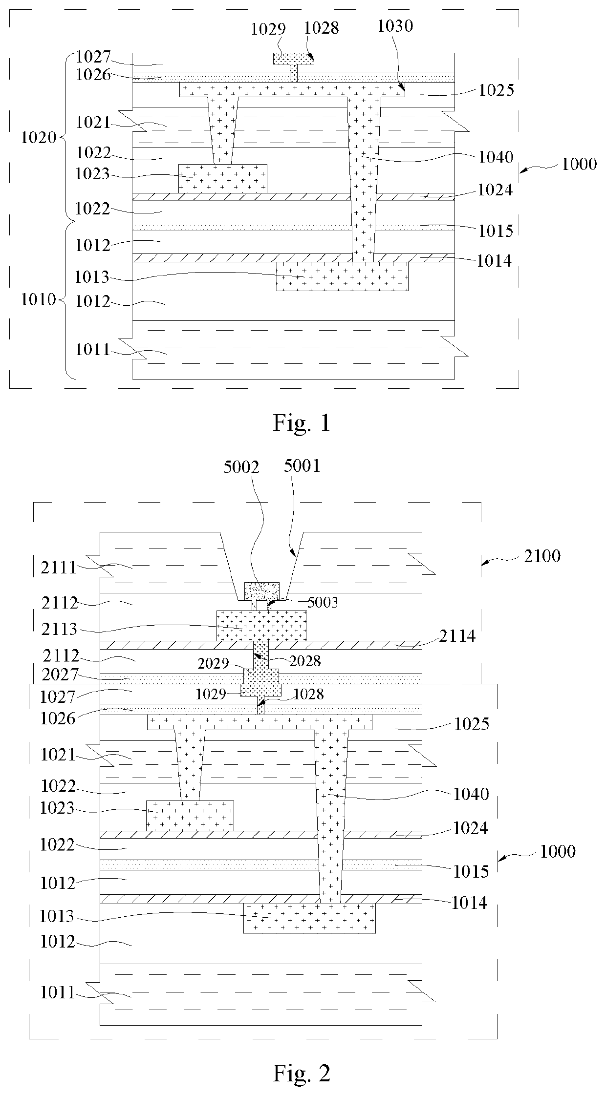
[0050]FIG. 1 is a cross-sectional schematic view of a first unit of this embodiment, and FIG. 2 is a cross-sectional schematic view of the multi-wafer bonding structure of this embodiment. As shown in FIG. 1 and FIG. 2, this embodiment provides a multi-wafer bonding structure, including a first unit 1000 and a second unit 2100 that are bonded to each other. The first unit 1000 includes an upper wafer of the first unit 1020 and a lower wafer of the first unit 1010 that are bonded together, and the second unit 2100 includes a second unit wafer. In this embodiment, the lower wafer of the first unit 1010, the upper wafer of the first unit 1020 and the second unit wafer are sequentially stacked from bottom to top, and the second unit wafer serves as the topmost wafer of the multi-wafer bonding structure.

[0051]Specifically, as shown in FIG. 1, the upper wafer of the first unit 1020 includes a substrate 1021, a dielectric layer 1022 located on a surface of the substrate 1021 and a metal la...

embodiment 2

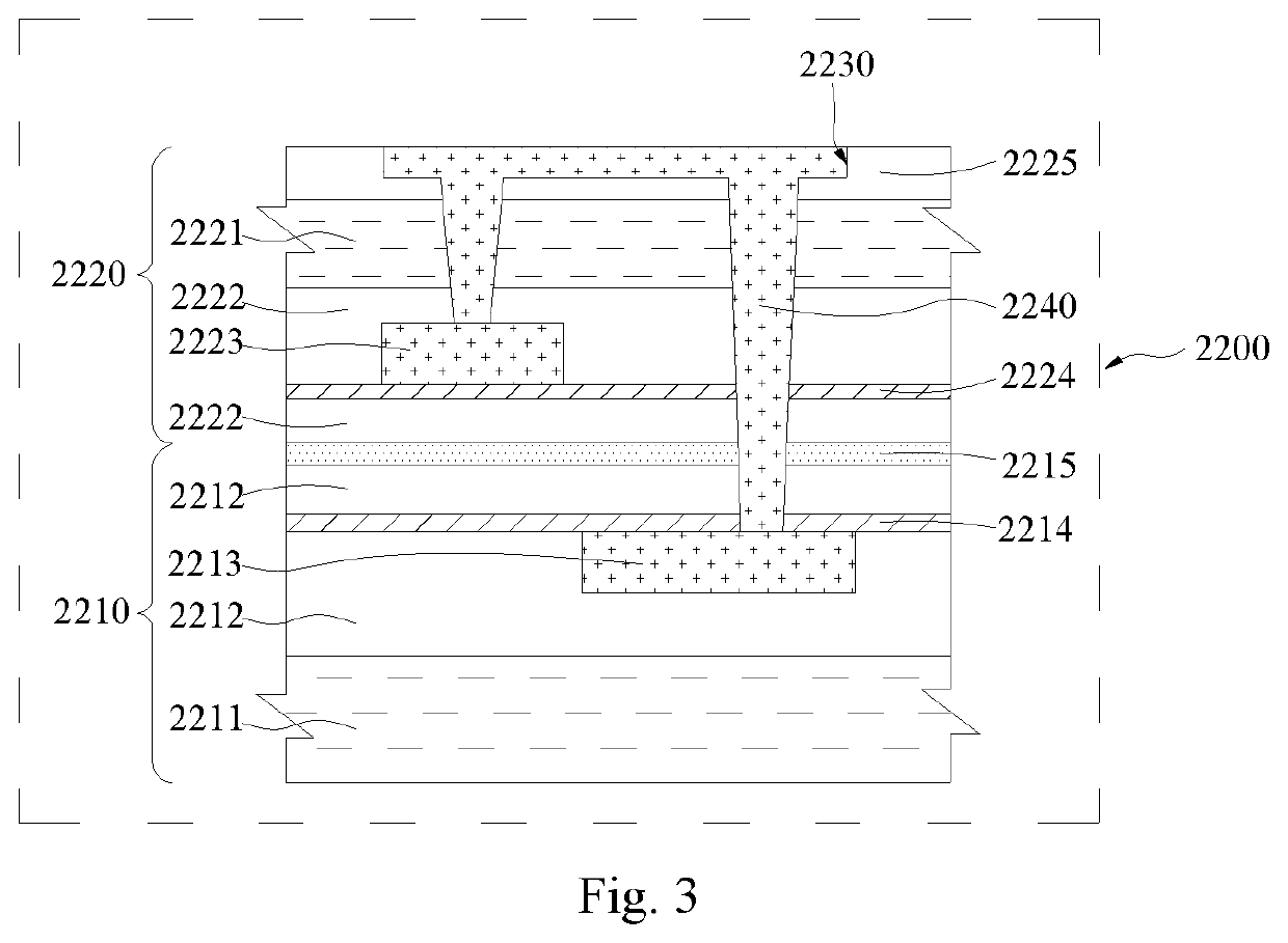
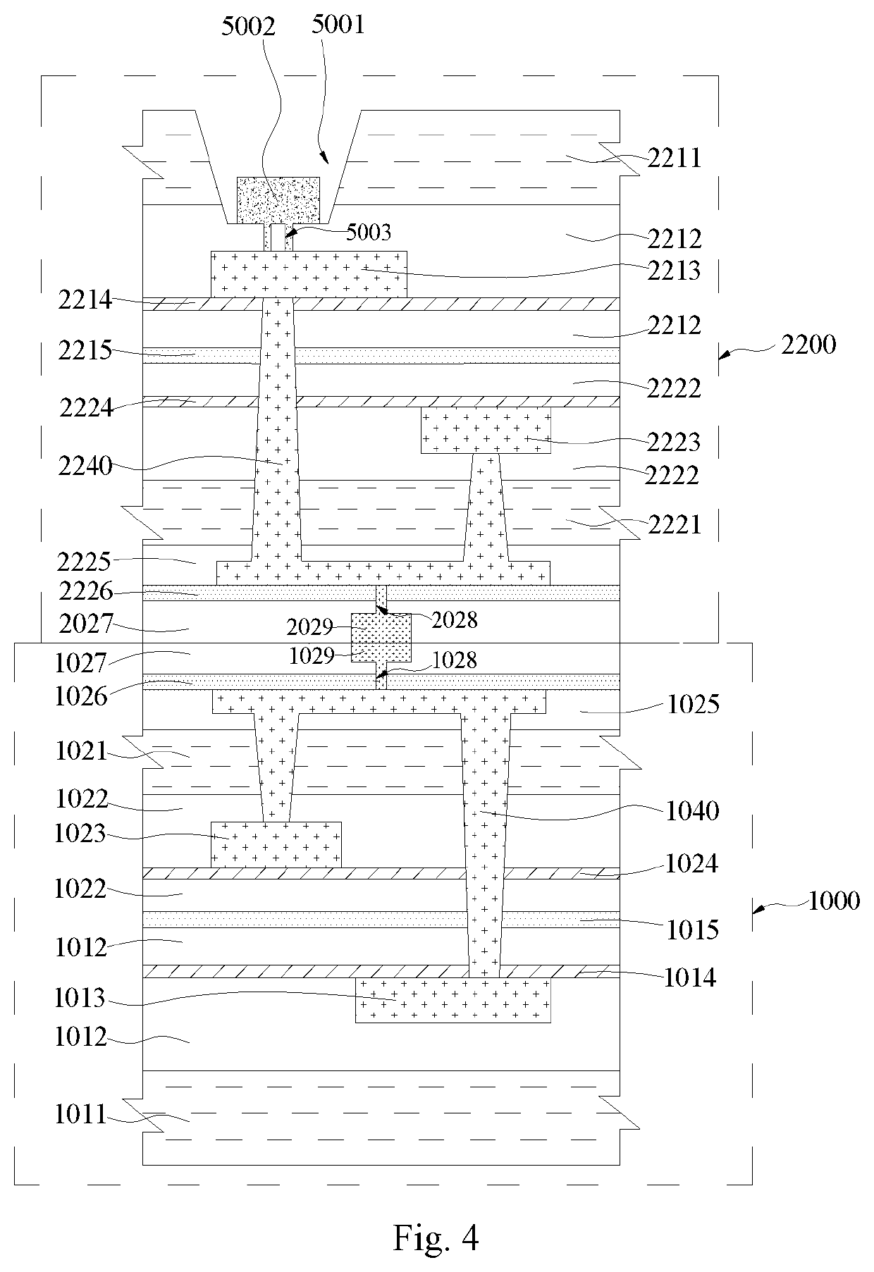
[0070]FIG. 3 is a cross-sectional schematic view of a second unit of this embodiment, and FIG. 4 is a cross-sectional schematic view of the multi-wafer bonding structure of this embodiment. As shown in FIG. 3 and FIG. 4, a multi-wafer bonding structure includes a first unit 1000 and a second unit 2200 that are bonded to each other. The first unit 1000 includes an upper wafer of the first unit 1020 and a lower wafer of the first unit 1010 that are bonded to each other. The second unit 2200 includes an upper wafer of the second unit 2220 and a lower wafer of the second unit 2210 that are bonded to each other. The upper wafer of the second unit 2220 and the upper wafer of the first unit 1020 are bonded to each other. In this embodiment, the lower wafer of the first unit 1010, the upper wafer of the first unit 1020, the upper wafer of the second unit 2220 and the lower wafer of the second unit 2210 are sequentially stacked from bottom to top. The lower wafer of the second unit 2210 serv...

embodiment 3

[0081]FIG. 5 is a cross-sectional schematic view of a multi-wafer bonding structure of this embodiment. As shown in FIG. 3 and FIG. 5, a multi-wafer bonding structure of this embodiment includes a first unit 1000, a second unit 2200 and a third unit 3000 that are bonded sequentially. The first unit 1000 includes an upper wafer of the first unit 1020 and a lower wafer of the first unit 1010 that are bonded together. The second unit 2200 includes an upper wafer of the second unit 2220 and a lower wafer of the second unit 2210 that are bonded to each other. The third unit 3000 includes a third unit wafer. The upper wafer of the second unit 2220 is bonded to the third unit wafer, and the lower wafer of the second unit 2210 and the upper wafer of the first unit 1020 are bonded to each other. In this embodiment, the lower wafer of the first unit 1010, the upper wafer of the first unit 1020, the lower wafer of the second unit 2210, the upper wafer of the second unit 2220 and the third unit...


PUM

PropertyMeasurementUnit
structureaaaaaaaaaa
electricalaaaaaaaaaa
dielectricaaaaaaaaaa

Abstract

A multi-wafer bonding structure and bonding method are disclosed. The multi-wafer bonding structure includes a first unit and a second unit, a metal layer of each wafer in the first unit electrically connected to an interconnection layer of the first unit, a first bonding layer in the first unit electrically connected to the interconnection layer of the first unit, a second bonding layer in the second unit electrically connected to a metal layer of the second unit, and the first bonding layer being in contact with the second bonding layer to achieve an electrical connection, thereby achieving the electrical connection among the interconnection layer of the first unit, the first bonding layer, the second bonding layer and the metal layer of each wafer.

Description

CROSS-REFERENCE TO RELATED APPLICATION[0001]This application claims the priority of Chinese patent application number 201810988451.9, filed on Aug. 28, 2018, the entire contents of which are incorporated herein by reference.TECHNICAL FIELD[0002]The present invention relates to the technical field of integrated circuit manufacturing and, in particular, to a multi-wafer bonding structure and bonding method.BACKGROUND[0003]In the trend of developing highly integrated semiconductors, a 3D packaging technology is an effective way to improve the integration level and a signal interconnection speed. There are two common 3D packaging methods: 1. chip stacking based on lead wire bonding, which achieves interconnection by external lead wires; 2. package-on-package, which achieves interconnection by soldering solder balls of the devices. However, the lead wire bonding of the chip stacking and the solder ball soldering of the package-on-package have the defects of long interconnection distance,...

Claims


Application Information

Patent Timeline
Patent Type & Authority Applications(United States)
IPC IPC(8): H01L25/065H01L25/00H01L23/00H01L23/48H01L21/768H01L21/027
CPCH01L2224/08146H01L21/76898H01L24/80H01L2225/06541H01L21/0274H01L23/481H01L24/08H01L23/562H01L2224/80894H01L2924/351H01L25/0657H01L25/50H01L2225/06524H01L23/5226H01L23/5283H01L21/76802H01L21/76877H01L23/3171H01L23/3192H01L2225/06544H01L2225/06513H01L2224/08145H01L24/05H01L2224/80896H01L2224/80895
Inventor YE, GUOLIANG
Owner WUHAN XINXIN SEMICON MFG CO LTD
Why Eureka
Try Eureka