Three-dimensional integrated cooling gain-type semiconductor assembly and fabrication method thereof

A semiconductor, gain-type technology, applied in the direction of semiconductor devices, semiconductor/solid-state device components, electric solid-state devices, etc., can solve the problems of low production qualification rate, complex process, high cost, etc., and achieve the effect of reliable connection channels

Inactive Publication Date: 2018-08-14
BRIDGE SEMICON
View PDF13 Cites 0 Cited by
  • Summary
  • Abstract
  • Description
  • Claims
  • Application Information

AI Technical Summary

Problems solved by technology

Although it does not require the formation of through-silicon vias (TSVs) in the stacked chips, the TSVs in the interposer used to provide electrical routing between chips will lead to complex processes, low production yield and high cost

Method used


Image

  • Three-dimensional integrated cooling gain-type semiconductor assembly and fabrication method thereof
  • Three-dimensional integrated cooling gain-type semiconductor assembly and fabrication method thereof
  • Three-dimensional integrated cooling gain-type semiconductor assembly and fabrication method thereof

Examples


Embodiment 1

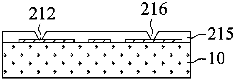
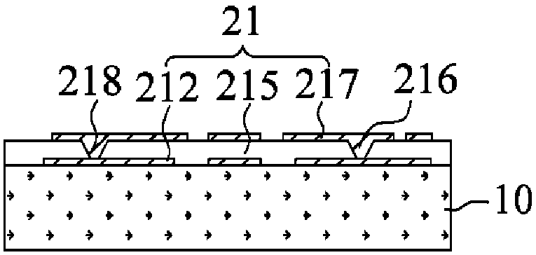
[0088] Figure 1-13 It is a diagram of a manufacturing method of a semiconductor component in the first embodiment of the present invention, which includes a first routing circuit 21, a first device 22, a molding material 25, a second device 27, a heat sink 30 and Bonding wires 41,43.

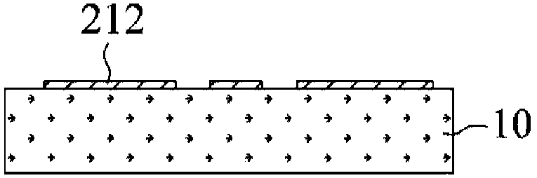
[0089] figure 1 It is a cross-sectional view of the routing lines 212 formed on the sacrificial carrier 10 . The sacrificial carrier 10 is typically made of copper, aluminum, iron, nickel, tin, stainless steel, silicon or other metals or alloys, but any other conductive or non-conductive material could also be used. In this embodiment, the sacrificial carrier 10 is made of ferrous material. Routing lines 212 are usually made of copper and can be patterned and deposited by various techniques, such as electroplating, electroless plating, evaporation, sputtering or a combination thereof, or formed by thin film deposition followed by a metal patterning step. As far as the conductive sacrificial...

Embodiment 2

[0114] Figure 18-20 In the second embodiment of the present invention, it is a diagram of a manufacturing method of a semiconductor device in which a second routing circuit is electrically coupled to a metal post.

[0115] For the purpose of brief description, any statements in the above-mentioned embodiment 1 that can be used for the same application are incorporated here, and there is no need to repeat the same statements.

[0116] Figure 18 It is a sectional view of the heat sink 30 . The heat sink 30 with Figure 11 The structures shown are similar, but the difference is that the second routing circuit 33 further includes a build-up insulating layer 361 and a fourth wire 364, wherein the build-up insulating layer 361 is laminated / coated on the routing substrate 351 and the metal pillars 323, 324 , and the fourth wire 364 is deposited on the build-up insulating layer 361 . The build-up insulating layer 361 contacts the routing substrate 351 and the metal pillars 323 ,...

Embodiment 3

[0125] Figure 24-27 It is a diagram of another method of manufacturing a semiconductor component in the third embodiment of the present invention, the metal plate has a through hole, and the through hole is aligned with the through opening of the second routing circuit.


PUM


Abstract

The invention relates to a three-dimensional integrated semiconductor assembly. The three-dimensional integrated semiconductor assembly comprises a face-to-face semiconductor secondary assembly and acooling seat, wherein the face-to-face semiconductor secondary assembly and the cooling seat are electrically coupled to each other by a bonding wire, the face-to-face semiconductor secondary assemblycomprises a top device and a bottom device, the top device and the bottom device are respectively connected to two sides, opposite to each other, of a first route circuit, the cooling seat comprisesa metal plate and a second route circuit, the second route circuit is arranged on the metal plate, the face-to-face semiconductor assembly is arranged in the cooling seat and in a penetrating openingof the second route circuit, the bonding wire is used for providing electrical connection between the first route circuit and the second route circuit, so that a device assembled into the secondary assembly in a face-to-face way is interconnected to a terminal cushion of the cooling seat.

Description

technical field [0001] The present invention relates to a semiconductor component and its manufacturing method, especially to a three-dimensionally integrated heat dissipation-enhanced semiconductor component, which electrically connects the face-to-face semiconductor sub-component to the heat sink through bonding wires. Background technique [0002] The market trend of multimedia devices tends to be faster and thinner. One of the methods is to interconnect two devices in a face-to-face manner so that the routing distance between the two devices is the shortest. Since stacked devices can directly communicate with each other to reduce delay, the signal integrity of components can be greatly improved and additional power consumption can be saved. Therefore, the face-to-face semiconductor device can exhibit almost all the advantages of 3D IC stacking, without the need to form costly through-silicon vias (Through-Silicon Via) in the stacked chips. However, since semiconductor ...

Claims


Application Information

Patent Timeline
Patent Type & Authority Applications(China)
IPC IPC(8): H01L23/31H01L23/367H01L23/498H01L23/522H01L23/528H01L25/07
CPCH01L2224/16225H01L2924/19107H01L23/3121H01L23/367H01L23/49816H01L23/522H01L23/528H01L25/071
Inventor 林文强王家忠
Owner BRIDGE SEMICON
Why Eureka
Try Eureka