Solid-state imaging device, method for driving solid-state imaging device, and electronic apparatus
a technology of solid-state imaging and imaging device, which is applied in the direction of color television details, television system details, television systems, etc., can solve the problem that the global shutter reading operation cannot be carried ou
- Summary
- Abstract
- Description
- Claims
- Application Information
AI Technical Summary
Benefits of technology
Problems solved by technology
Method used
Image
Examples
first embodiment
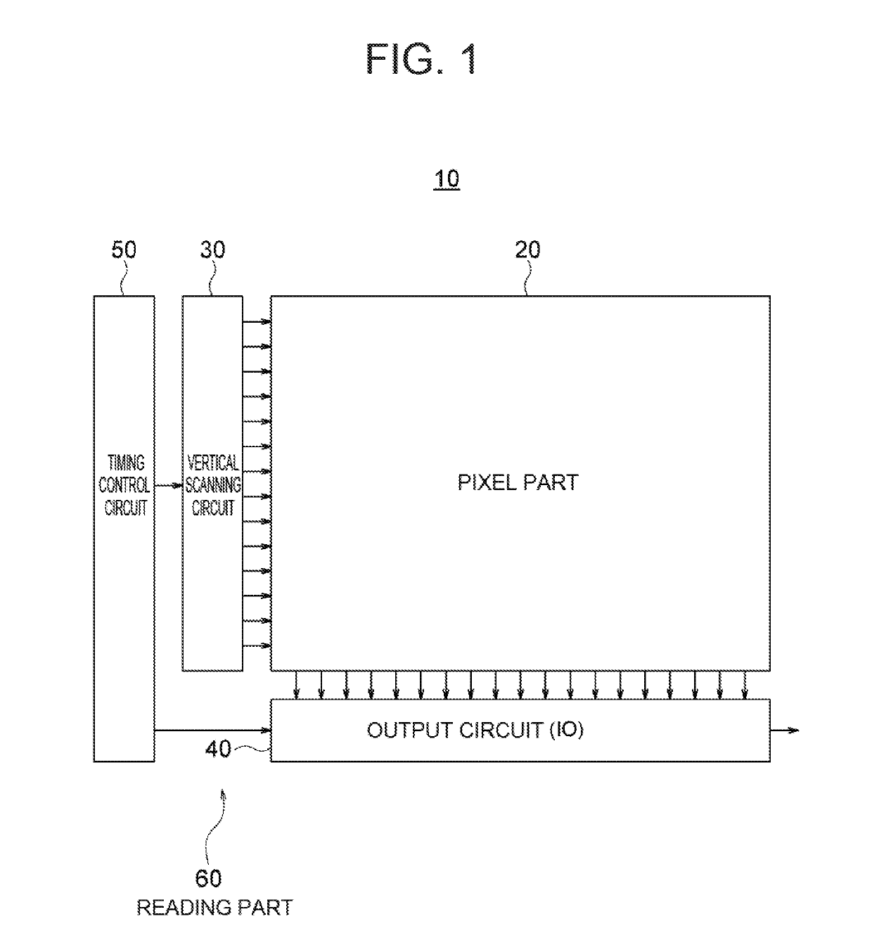
[0042]FIG. 1 is a block diagram showing an example of the configuration of a solid-state imaging device according to a first embodiment of the present invention. In the present embodiment, a solid-state imaging device 10 is constituted by for example a CMOS image sensor including digital pixels as the pixels.
[0043]As shown in FIG. 1, the solid-state imaging device 10, is constituted mainly by an image capturing part constituted by a pixel part 20, a vertical scanning circuit (row scanning circuit) 30, an output circuit 40, and a timing control circuit 50. Among these components, for example, the vertical scanning circuit 30, the output circuit 40, and the timing control circuit 50 constitute the reading part 60 for reading out pixel signals.
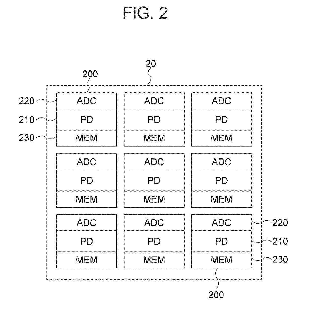
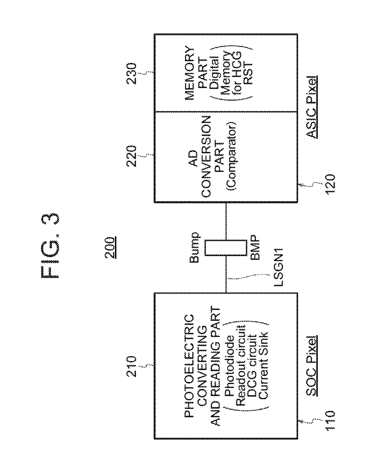
[0044]In the first embodiment, the solid-state imaging device 10 is configured as for example a stacked type CMOS image sensor which, in the pixel part 20, includes digital pixels comprised of photoelectric converting and reading parts, AD (analo...
second embodiment
[0129]FIG. 11A and FIG. 11B are block diagrams showing an example of the configuration of a digital pixel in a solid-state imaging device according to a second embodiment of the present invention. FIG. 12 is a circuit diagram showing an example of the configuration of the digital pixel according to the second embodiment of the present invention. FIG. 13 is a circuit diagram showing an example of the configuration of a photoelectric converting and reading part in the digital pixel according to the second embodiment of the present invention. FIG. 14 is a circuit diagram showing an example of the configurations of an AD conversion part and a memory part in the digital pixel according to the second embodiment of the present invention.
[0130]The difference of a solid-state imaging device 10A according to the second embodiment from the solid-state imaging device 10 according to the first embodiment explained above is as follows. In the solid-state imaging device 10A according to the second...
third embodiment
[0139]FIG. 19 is a block diagram showing an example of the configuration of a digital pixel in a solid-state imaging device according to a third embodiment of the present invention. FIG. 20 is a circuit diagram showing an example of the configuration of the digital pixel according to the third embodiment of the present invention
[0140]The difference of a solid-state imaging device 10B according to the third embodiment from the solid-state imaging device 10 according to the first embodiment explained above is as follows In the solid-state imaging device 10B according to the third embodiment, the output of the comparator 221 is connected to a vertical signal line LSGN11 laid in units of columns, while a memory part 230B is arranged in units of columns and is connected to the vertical signal line LSGN11.
[0141]In the example in FIG. 19, a driver 222 and switch element SW220 are connected between the output side of the comparator 221 and the vertical signal line LSGN11.
[0142]The output of...
PUM
 Abstract
Description
Claims
Application Information
 - R&D
- Intellectual Property
- Life Sciences
- Materials
- Tech Scout
- Unparalleled Data Quality
- Higher Quality Content
- 60% Fewer Hallucinations
Browse by: Latest US Patents, China's latest patents, Technical Efficacy Thesaurus, Application Domain, Technology Topic, Popular Technical Reports.
© 2025 PatSnap. All rights reserved.Legal|Privacy policy|Modern Slavery Act Transparency Statement|Sitemap|About US| Contact US: help@patsnap.com


