Active matrix organic light emitting diode (AMOLED) display panel and recovery method thereof

A technology of a display panel and a repair method, which is applied to electrical components, electrical solid-state devices, circuits, etc., can solve problems such as abnormal pixel Px display and defective AMOLED display panels, and achieve the effect of improving yield

Inactive Publication Date: 2018-06-15
WUHAN CHINA STAR OPTOELECTRONICS SEMICON DISPLAY TECH CO LTD
View PDF11 Cites 3 Cited by
  • Summary
  • Abstract
  • Description
  • Claims
  • Application Information

AI Technical Summary

Problems solved by technology

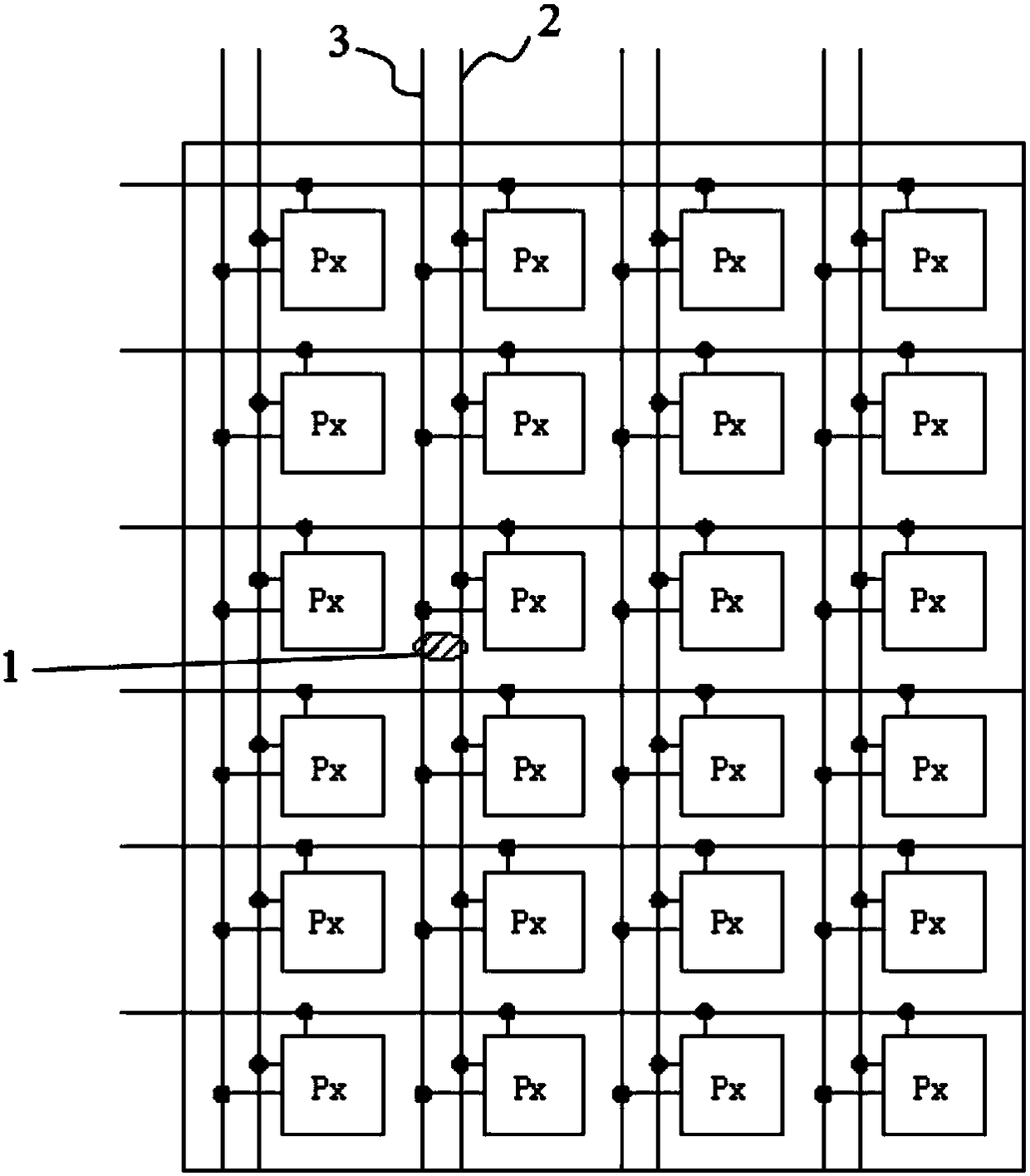
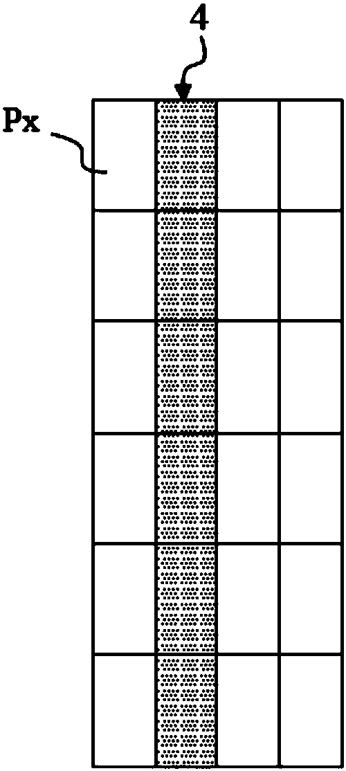
A short circuit in the data line 2 will cause an abnormality in the display of a whole column of pixels Px connected to the data line 2, such as figure 2 As shown, line defects 4 (corresponding to a whole column of pixels) are formed in the display screen. Such defects are unacceptable, and AMOLED display panels with line defects 4 will be judged as defective products

Method used


Image

  • Active matrix organic light emitting diode (AMOLED) display panel and recovery method thereof
  • Active matrix organic light emitting diode (AMOLED) display panel and recovery method thereof
  • Active matrix organic light emitting diode (AMOLED) display panel and recovery method thereof

Examples


Embodiment Construction

[0025] In order to make the object, technical solution and advantages of the present invention clearer, the specific implementation manners of the present invention will be described in detail below in conjunction with the accompanying drawings. Examples of these preferred embodiments are illustrated in the accompanying drawings. The embodiments of the invention shown in and described with reference to the drawings are merely exemplary, and the invention is not limited to these embodiments.

[0026] Here, it should also be noted that, in order to avoid obscuring the present invention due to unnecessary details, only the structures and / or processing steps closely related to the solution according to the present invention are shown in the drawings, and the related Other details are not relevant to the invention.

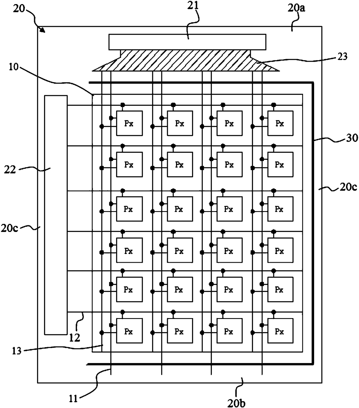
[0027] This embodiment provides an AMOLED display panel, such as image 3 As shown, the AMOLED display panel includes a display area 10 and a peripheral circuit area...


PUM


Abstract

The invention discloses an active matrix organic light emitting diode (AMOLED) display panel and a recovery method thereof. The AMOLED display panel comprises a display region and a peripheral circuitregion, wherein a data line is arranged in the display region, the peripheral circuit region comprises a first region, a second region and a third region, one end of the data line extends to a firstregion, the other end of the data line extends to a second region, a recovery line is arranged in the peripheral circuit region and extends to the second region from the first region to the third region, the recovery line is in insulation intersection with the data line in the first region, the recovery line is in insulation intersection with the data line in the second region, and the recovery line is configured to recovery the data line when the data line is circuit-shorted in the display region. By the AMOLED display panel, the unfavorable data line with short circuit can be recovered, a pixel with abnormal display in a display image is reduced to be within an acceptable range, and the final product yield is improved.

Description

technical field [0001] The invention relates to the technical field of displays, in particular to an AMOLED display panel and a repair method thereof. Background technique [0002] Flat panel displays are widely used in various electronic products such as TVs, computers, tablet computers and smart phones, and play a pivotal role in the electronic information industry. As an emerging representative of flat panel display, AMOLED (Active Matrix Organic Light Emitting Diode, active matrix organic light emitting diode) display panel has the advantages of self-illumination, wide viewing angle, bright color, high contrast, wide operating temperature range and suitable for flexible display. To develop rapidly. [0003] The AMOLED display panel includes criss-crossing data lines and scanning lines, and also includes a pixel structure located at the crossing area of ​​the data lines and the scanning lines, and a plurality of pixel structures are arranged in a matrix array. A typical...

Claims


Application Information

Patent Timeline
Patent Type & Authority Applications(China)
IPC IPC(8): H01L27/32
CPCH10K59/131H10K59/1201
Inventor 易士娟
Owner WUHAN CHINA STAR OPTOELECTRONICS SEMICON DISPLAY TECH CO LTD
Why Eureka
Try Eureka