System and method for controlling phase allignment of clock signals

a phase alignment and clock signal technology, applied in the field of integrated circuits, can solve the problems of inability to incorporate regular ddr dram segments into the umbrella of operation, method might not produce accurate end-results in terms of path replication

Active Publication Date: 2019-02-28
SYNOPSYS INC
View PDF2 Cites 3 Cited by
  • Summary
  • Abstract
  • Description
  • Claims
  • Application Information

AI Technical Summary

Benefits of technology

The patent text describes a system and method to improve the accuracy of aligning phases. Additionally, it simplifies the physical implementation of aDDR DRAM controller by reducing the strict path matching between widely distributed cells.

Problems solved by technology

There is also a probability that the aforementioned factors create a mismatch between a clock signal (CLK) and the corresponding command signals (CMD) generated by DDR DRAM controller.
At least some of the well known calibration techniques require active feedback from the DDR DRAM memory, and are restricted at least in terms of implementation to low power DDR DRAM modules.
The drawbacks of the aforementioned calibration include inter-alia excessive dependence on the feedback received from DDR DRAM, and the inability to incorporate regular DDR DRAM segments into its umbrella of operation.
However, the aforementioned conventional method might not produce accurate end-results in terms of path replication due to variations witnessed across the actual path and the replica path.
Further, another disadvantage associated with the aforementioned technique is the difficulty involved in physical implementation of the replica path on an IC.

Method used


Image

  • System and method for controlling phase allignment of clock signals
  • System and method for controlling phase allignment of clock signals
  • System and method for controlling phase allignment of clock signals

Examples


Embodiment Construction

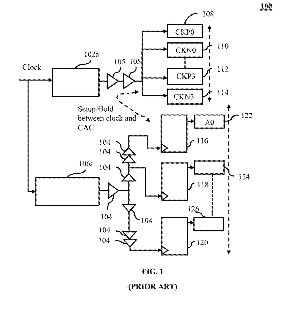
[0021]Referring to FIG. 1, there is shown an illustration of the clock and command network distribution of a conventional DDR DRAM controller. Referring to FIG. 1, the clock and command network 100 is bifurcated primarily into a clock section 102 and Command Address Control (CAC) section 106. In accordance with the present disclosure, a clock signal is simultaneously transmitted to a first Slave Delay Lock Loop (SDLL) 102a, and to the second Slave Delay Lock Loop (SDLL) 106a.

[0022]In accordance with the present disclosure, the clock section 102 includes a plurality of differential pads represented by reference numerals 108, 110, 112 and 114 respectively. Further, the command, address and control (CAC) section 106 includes a plurality of single ended pads represented by reference numerals 122, 124 and 126 respectively. A plurality of buffer circuits represented by reference numeral 104 and 105 respectively, route the clock signal to the differential pads 108, 110, 112 and 114 and th...


PUM


Abstract

A system and method for aligning clock signals in a DDR DRAM module is disclosed. The system includes a phase detector circuitry, a controllable delay circuit, a first delay circuit and a synchronizing circuit. A clock signal is simultaneously transmitted through the first delay circuit and the controllable delay circuit. Subsequently, the clock signals transmitted through the first delay circuit and the controllable delay circuit are captured at the output thereof, and fed as inputs to the phase detector circuitry. The phase detector circuitry determines whether the clock signals are in phase, and accordingly adjusts the delay associated with the controllable delay circuit until the two clock signals are determined to be in phase.

Description

CROSS REFERENCE TO RELATED APPLICATIONS[0001]This Patent Application is a National Phase Application corresponding to the PCT Application No. PCT / IN2016 / 000170 filed on Jun. 30, 2016 with the title “SYSTEM AND METHOD FOR CONTROLLING PHASE ALLIGNMENT OF CLOCK SIGNALS”. This Patent Application claims the priority of the Indian Provisional Patent Application No. 1782 / CHE / 2015 filed on Jul. 03, 2015 with the title “A SYSTEM AND METHOD FOR PHASE ALIGNMENT OF CLOCK AND COMMAND FOR DDR DRAM CONTROLLER”, the contents of which is included herein by the way of reference.BACKGROUNDTechnical Field[0002]The present disclosure generally relates to integrated circuits. Particularly, the present disclosure relates to phase alignment of signals in an integrated circuit. More particularly, the present disclosure relates to phase alignment of signals in a DDR DRAM system.Description of the Related Art[0003]During the designing of an integrated circuit, due emphasis is to be provided for precise delay ...

Claims


Application Information

Patent Timeline
IPC IPC(8): G11C7/10H03L7/081H03L7/091G11C7/22G11C8/06
CPCG11C7/1093H03L7/0812H03L7/091G11C7/109G11C7/222G11C8/06H03L7/00H03L7/0814G06F1/10H03L7/0816
Inventor PRAKASH, GYANKUMAR, NIDHIRVORUGU, MUNISWARA REDDY
Owner SYNOPSYS INC
Why Eureka
Try Eureka