Semiconductor element test apparatus and semiconductor element test method
a test apparatus and semiconductor technology, applied in the direction of electronic circuit testing, measurement devices, instruments, etc., can solve the problems of promoting damage to test instruments, so as to reduce the damage of test instruments and restrict the flow of current through the semiconductor elements.
- Summary
- Abstract
- Description
- Claims
- Application Information
AI Technical Summary
Benefits of technology
Problems solved by technology
Method used
Image


Examples
first embodiment
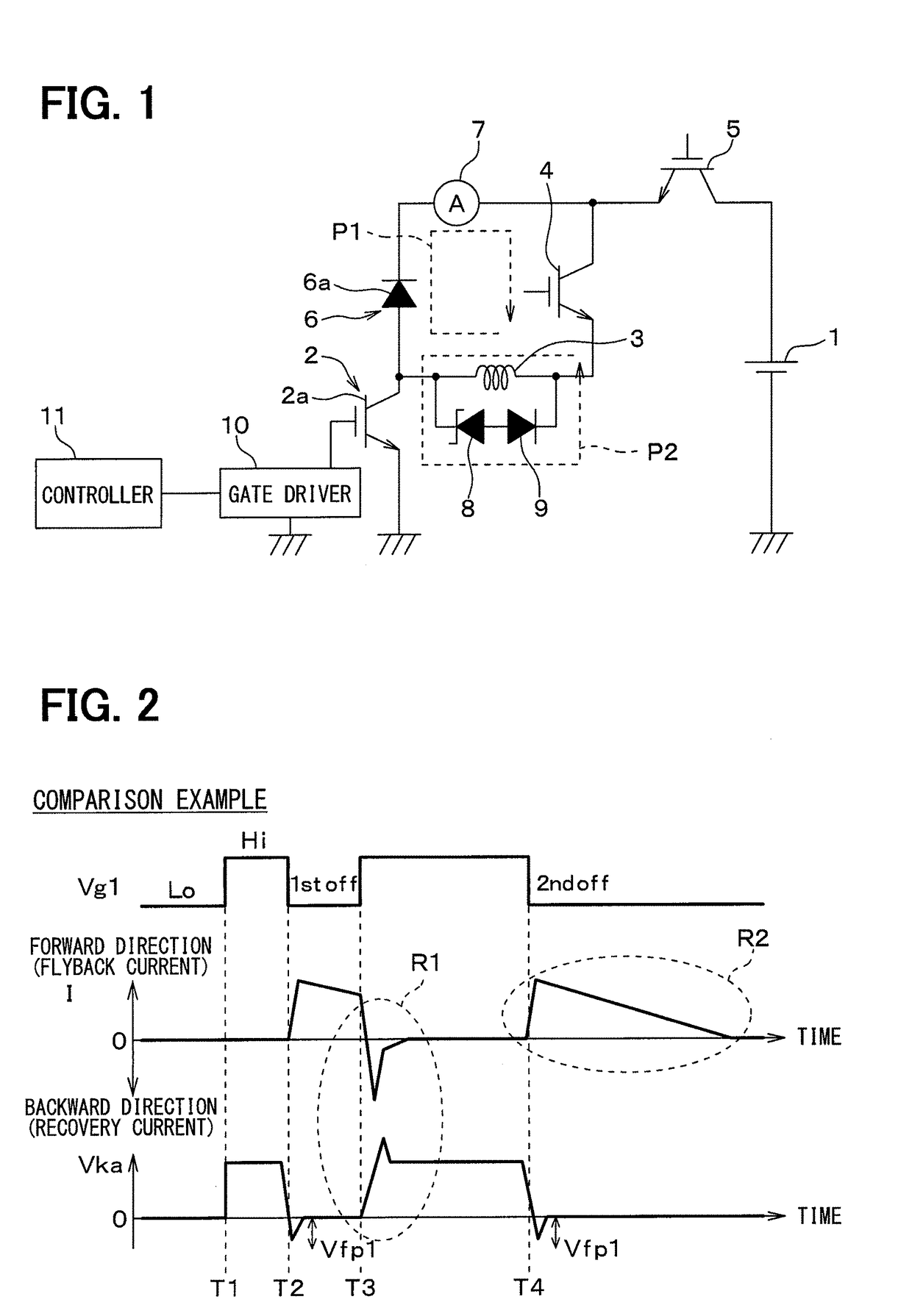
[0024]A first embodiment of the present disclosure will be described. A semiconductor element test apparatus according to the present embodiment performs a recovery test of a semiconductor element by employing a power source 1. As shown in FIG. 1, the test apparatus of the present embodiment includes the power source 1, a first switch 2, a coil 3, a second switch 4, a protection switch 5, a DUT 6, an ammeter 7, a first rectifying element 8, a second rectifying element 9, a gate driver 10, and a controller 11.
[0025]As shown in FIG. 1, the protection switch 5, the second switch 4, the coil 3, and the first switch 2 are connected in series to the power source 1. The first switch 2 switches a path of current that flows through the coil 3. In the present embodiment, the first switch 2 has a switching element 2a. The switching element 2a is provided by an N channel IGBT (Insulated Gate Bipolar Transistor) element having a gate electrode, a collector electrode, and an emitter electrode.
[00...
second embodiment
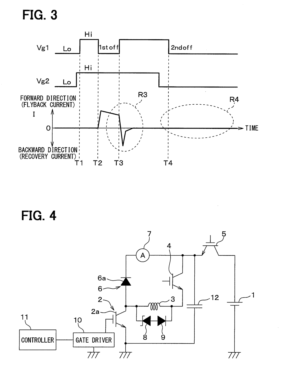
[0068]Hereinafter, a second embodiment of the present disclosure will be described. In the present embodiment, a protect element 13 is added to the first embodiment. Other parts are same as the parts of the first embodiment. Thus, only a part of a configuration that is different from the configuration of the first embodiment will be described.
[0069]As shown in FIG. 6, in the present embodiment, the protect element 13 is disposed to configure a loop path along with the coil 3, the second switch 4, the DUT 6, and the ammeter 7 when the first switch 2 is switched off. The protect element 13 has a protect diode element 13a having larger breakdown strength than the DUT 6.
[0070]The protect diode element 13a is provided by the FWD element, and disposed to have the same rectification direction as the diode element 6a. A cathode electrode of the protect diode element 13a is connected to the anode electrode of the diode element 6a. An anode electrode of the protect diode element 13a is connec...
third embodiment
[0075]A third embodiment of the present disclosure will be described. In the present embodiment, an upper arm drive (that is, a high side drive) replaces a lower arm drive (that is, a low side drive) provided by the protect element 13 in the second embodiment. Other parts are same as the parts of the second embodiment. Thus, only a part of a configuration that is different from the configuration of the second embodiment will be described.
[0076]In the present embodiment, positions of elements configuring the loop path P1 are exchanged with a position of the first switch 2. As shown in FIG. 7, the emitter electrode of the protection switch 5 is connected to the collector electrode of the switching element 2a, and the emitter electrode of the switching element 2a is connected to the cathode electrode of the protect diode element 13a. Voltage of the emitter electrode of the switching element 2a is input to the gate driver 10.
[0077]The anode electrode of the protect diode element 13a is ...
PUM
 Abstract
Description
Claims
Application Information
 - R&D
- Intellectual Property
- Life Sciences
- Materials
- Tech Scout
- Unparalleled Data Quality
- Higher Quality Content
- 60% Fewer Hallucinations
Browse by: Latest US Patents, China's latest patents, Technical Efficacy Thesaurus, Application Domain, Technology Topic, Popular Technical Reports.
© 2025 PatSnap. All rights reserved.Legal|Privacy policy|Modern Slavery Act Transparency Statement|Sitemap|About US| Contact US: help@patsnap.com