Method for manufacturing semiconductor device, semiconductor mounting device, and memory device manufactured by method for manufacturing semiconductor device

a manufacturing method and semiconductor technology, applied in semiconductor devices, semiconductor/solid-state device details, electrical devices, etc., can solve the problems of increasing mounting time and reducing the bonding defect between the substrate and the semiconductor, so as to shorten the manufacturing time, improve the cutting accuracy of the cutting means, and manufacture a semiconductor device

Active Publication Date: 2018-04-05
TORAY ENG CO LTD
View PDF3 Cites 7 Cited by
  • Summary
  • Abstract
  • Description
  • Claims
  • Application Information

AI Technical Summary

Benefits of technology

[0015]In the present invention, a plurality of chip parts are laminated all at once, and the main pressure bonding is performed after this laminate has been cut into provisional pressure-bonded laminate chip parts, so voids are less likely to occur. Also, reducing the gap between the semiconductor wafers makes it less likely that the semiconductor wafers will become misaligned during cutting. This shortens how long it takes to manufacture a semiconductor device in which chip parts are laminated and also makes it less likely that there will be joining defects between chip parts. Also, when chip parts are provisionally pressure bonded one at a time as is done conventionally, if the chip parts are thin the adhesive may bulge out and contaminate the tops of the chip parts or attachments, but with the present invention, the lamination can be performed as wafers, so a provisional pressure-bonded laminate with no bulging of the adhesive after provisional pressure bonding can be formed.
[0016]In the present invention, the cutting accuracy of the cutting means is improved and the effect that the cutting means has on the pressure-bonded laminate is kept to a minimum. Consequently, how long it takes to manufacture a semiconductor device in which the chip parts are laminated can be shortened, and joining defects between chip parts and the like will be less likely to occur.
[0017]In the present invention, the cutting accuracy of the dicing blade is improved and the effect that the dicing blade has on the pressure-bonded laminate is kept to a minimum. Consequently, how long it takes to manufacture a semiconductor device in which the chip parts are laminated can be shortened, and joining defects between chip parts and the like will be less likely to occur.
[0018]In the present invention, the occurrence of voids is suppressed. Consequently, how long it takes to manufacture a semiconductor device in which the chip parts are laminated can be shortened, and joining defects between chip parts and the like will be less likely to occur.
[0019]In the present invention, occurrence of warping or the like of the semiconductor wafers is suppressed. Consequently, how long it takes to manufacture a semiconductor device in which the chip parts are laminated can be shortened, and joining defects between chip parts and the like will be less likely to occur.
[0020]In the present invention, defective products other than joining defects are expelled. Consequently, how long it takes to manufacture a semiconductor device in which the chip parts are laminated can be shortened, and joining defects between chip parts and the like will be less likely to occur.

Problems solved by technology

This diminishes bonding defects between the substrate and the semiconductor parts and between the laminated semiconductors.
However, a drawback to the technique described in Patent Literature 1 is that the mounting time increases as the number of laminations and the number of mounting sites of the semiconductor parts increase.

Method used


Image

  • Method for manufacturing semiconductor device, semiconductor mounting device, and memory device manufactured by method for manufacturing semiconductor device
  • Method for manufacturing semiconductor device, semiconductor mounting device, and memory device manufactured by method for manufacturing semiconductor device
  • Method for manufacturing semiconductor device, semiconductor mounting device, and memory device manufactured by method for manufacturing semiconductor device

Examples


Embodiment Construction

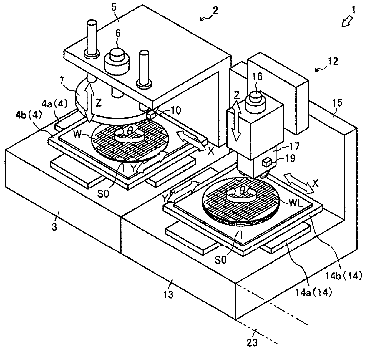
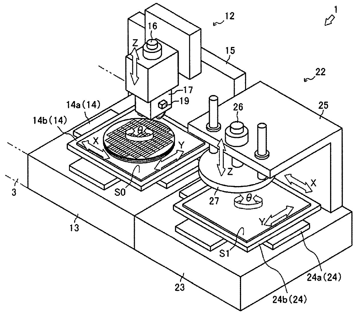
[0035]First, a semiconductor mounting device 1 that is an embodiment of the semiconductor mounting device pertaining to the present invention will be described through reference to FIGS. 1 to 4. In the following description, the direction in which the semiconductor wafer W is conveyed from a provisional pressure bonding device 2 to a main pressure bonding device 22 will be referred to as the X axis direction, the movement direction of a provisional pressure bonding head 7, a cutting head 17, and a main pressure bonding head 27 perpendicular to the semiconductor wafer W will be referred to as the Z axis direction, and the direction of rotation around the Z axis will be referred to as the θ direction. In this embodiment, the provisional pressure bonding device 2, a cutting device 12, and the main pressure bonding device 22 are each configured as an embodiment of the semiconductor mounting device 1, but the present invention is not limited to or by these.

[0036]A plurality of chip parts...


PUM


Abstract

A method for manufacturing a semiconductor device includes laminating a plurality of semiconductor wafers via an adhesive, heating such that the adhesive reaches a specific viscosity, and pressing the semiconductor wafers under a provisional pressure bonding load such that a gap between solder of through-electrodes provided to chip parts and through-electrodes of an adjacent semiconductor wafer falls within a specific range that is greater than zero, to produce a provisional pressure-bonded laminate; cutting the provisional pressure-bonded laminate with a cutter to produce a provisional pressure-bonded laminate chip part; and heating the provisional pressure-bonded laminate chip part to at least curing temperature of the adhesive and at least melting point of the solder, and pressing the provisional pressure-bonded laminate chip part under a main pressure bonding load to produce a main pressure-bonded laminate chip part such that the solder comes into contact with the through-electrodes of adjacent chip parts.

Description

[0001]This application is a U.S. National stage of International Application No. PCT / JP2016 / 060079 filed on Mar. 29, 2016. This application claims priority to Japanese Patent Application No. 2015-069740 filed with Japan Patent Office on Mar. 30, 2015. The entire disclosure of Japanese Patent Application No. 2015-069740 is hereby incorporated herein by reference.BACKGROUNDField of the Invention[0002]The present invention relates to a method for manufacturing a semiconductor device and to a semiconductor mounting apparatus. More particularly, the present invention relates to a method for manufacturing a semiconductor device in which a plurality of semiconductor wafers on which chip parts have been formed are laminated and electrically connected, to a semiconductor mounting apparatus, and to a memory device manufactured by a method for manufacturing a semiconductor device.Background Information[0003]Conventionally, in order to accommodate higher precision and miniaturization of a patte...

Claims


Application Information

Patent Timeline
Patent Type & Authority Applications(United States)
IPC IPC(8): H01L25/00H01L21/78H01L23/00
CPCH01L25/50H01L21/78H01L24/94H01L24/92H01L2224/16145H01L2224/94H01L24/13H01L24/16H01L24/29H01L24/32H01L24/73H01L24/81H01L24/83H01L2224/05571H01L2224/13009H01L2224/13082H01L2224/13116H01L2224/2919H01L2224/32145H01L2224/73104H01L2224/73204H01L2224/75252H01L2224/81203H01L2224/81815H01L2224/83191H01L2224/83203H01L2224/83862H01L2224/83907H01L2224/9205H01L2224/7598H01L25/0657H01L2225/06513H01L2225/06541H01L2225/06565B28D5/029H01L21/67092H01L21/67144H01L2224/8385H01L2224/9211H01L2224/81H01L2224/83H01L2924/00014H01L2924/00
Inventor ASAHI, NOBORUARAI, YOSHIYUKIMIYAMOTO, YOSHINORIAOKI, SHIMPEINIMURA, MASATSUGU
Owner TORAY ENG CO LTD
Why Eureka
Try Eureka