Manufacturing method for package device

Inactive Publication Date: 2018-07-19
DISCO CORP
View PDF16 Cites 1 Cited by
  • Summary
  • Abstract
  • Description
  • Claims
  • Application Information

AI Technical Summary

Benefits of technology

This patent aims to provide a method for making a package device. The method helps to prevent the electrode portion from being covered with adhesive, which can increase manufacturing time. The technical effect is to improve the efficiency of the manufacturing process.

Problems solved by technology

However, the adhesive layer configured by applying adhesive in the form of liquid as disclosed in Japanese Patent No. 5479866 has comparatively high flexibility in comparison with a DAF in the form of a film, and therefore is likely to spread around by pressure upon adhesion, and there is the possibility that the adhesive layer may cover also an electrode pad of a mounting substrate.

Method used


Image

  • Manufacturing method for package device
  • Manufacturing method for package device
  • Manufacturing method for package device

Examples


first embodiment

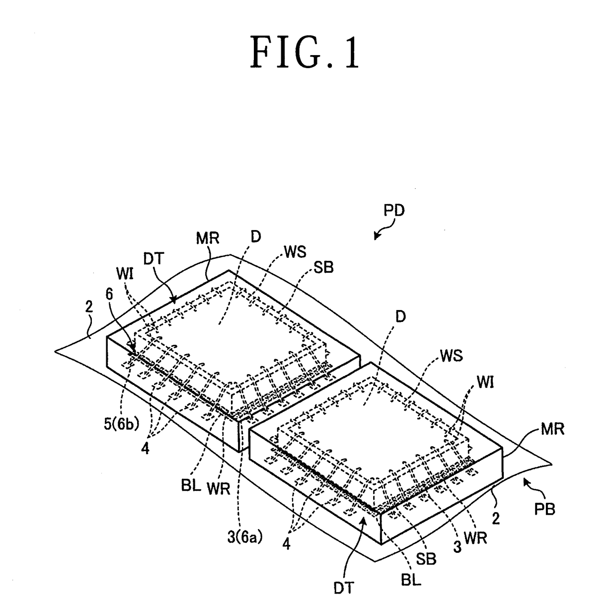
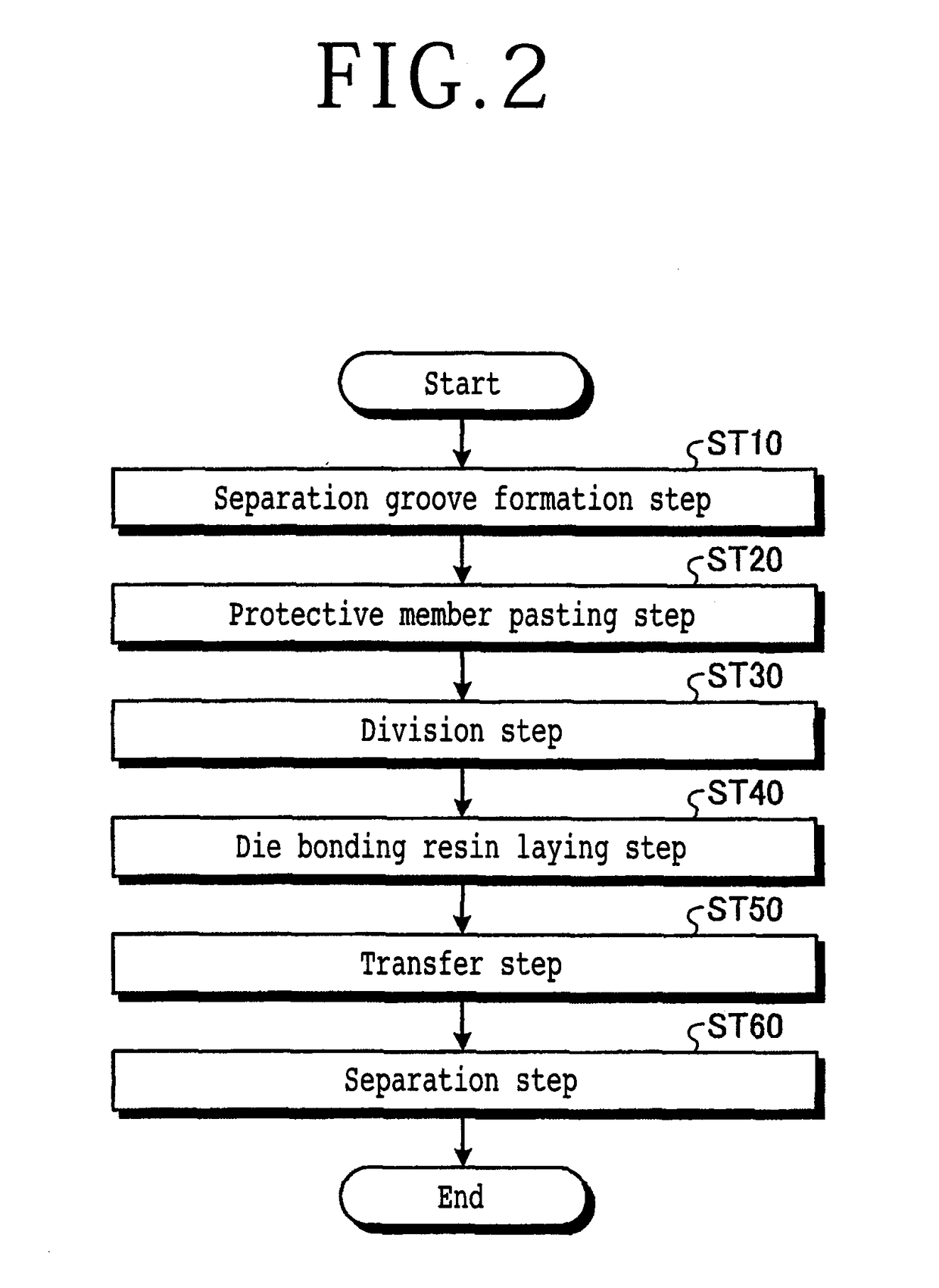
[0038]A manufacturing method for a package device according to a first embodiment is described with reference to the drawings. FIG. 1 is a perspective view depicting part of a package device manufactured by the manufacturing method for a package device according to the first embodiment.

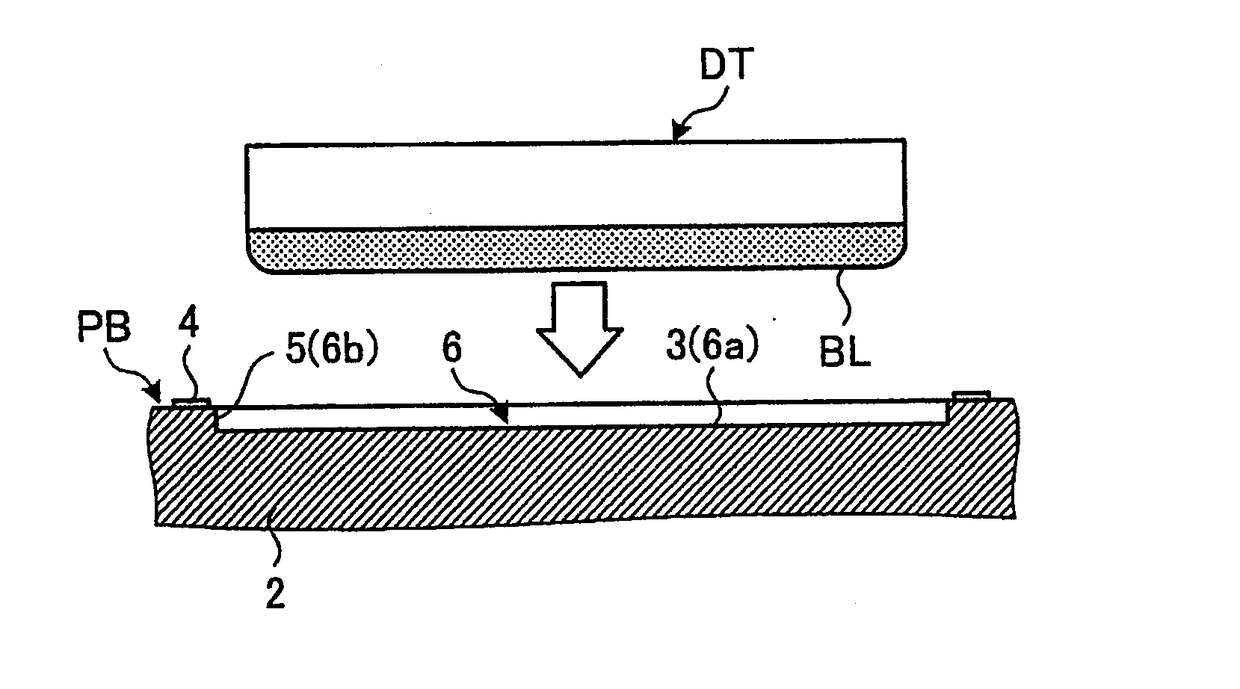
[0039]The manufacturing method for a package device according to the first embodiment is a method for manufacturing a package device PD depicted in FIG. 1. The package device PD includes a device chip DT, a mounting substrate PB on which the device chip DT is mounted, and mold resin MR as depicted in FIG. 1.

[0040]The device chip DT includes a substrate SB, a device D provided on a front face WS of the substrate SB, and an adhesive layer BL provided on a rear face WR that is one face of the substrate SB. The device D is an electronic part such as an integrated circuit (IC), a large-scale integration (LSI) or the like. Although, in the first embodiment, the device D of the device chip DT is a control de...

second embodiment

[0068]Now, a manufacturing method for a package device PD according to a second embodiment is described with reference to the drawings. FIG. 15 is a perspective view depicting a mounting step of the manufacturing method for a package device according to the second embodiment. FIG. 16 is a sectional view depicting the mounting step of the manufacturing method for a package device according to the second embodiment. FIG. 17 is a sectional view depicting a hardening step of the manufacturing method for a package device according to the second embodiment. FIG. 18 is a sectional view depicting a connection step of the manufacturing method for a package device according to the second embodiment. FIG. 19 is a sectional view depicting a molding step of the manufacturing method for a package device according to the second embodiment. In FIGS. 15 to 19, like elements to those in the first embodiment are denoted by like reference symbols and description of them is omitted.

[0069]The manufacturi...

third embodiment

[0074]Now, a manufacturing method for a package device PD according to a third embodiment is described with reference to the drawing. FIG. 20 is a sectional view depicting a package device manufactured by a manufacturing method for a package device according to a third embodiment. In FIG. 20, like elements to those in the first embodiment are denoted by like reference symbols and description of them is omitted.

[0075]The third embodiment is similar to the first embodiment except that the chip adhesion region 3 of the package device PD is an upper face 8a of a projected portion 8 formed so as to be projected from the front face of the substrate 2 and the stepped portion 5 has an outer side face 8b orthogonal to the upper face 8a that is the chip adhesion region 3 as depicted in FIG. 20. An angular portion that is a connection portion between the outer side face 8b and the chip adhesion region 3 acts to suppress adhesive, which configures an adhesive layer BL, from leaking to the outer...


PUM


Abstract

A manufacturing method for a package device includes a chip preparation step of preparing a device chip that includes an adhesive layer, a mounting substrate preparation step of preparing a mounting substrate that has a chip adhesion region to which the device chip is to be adhered, an electrode portion to be connected to the device chip, and a stepped portion formed between the chip adhesion region and the electrode portion, a mounting step of adhering the device chip to the chip adhesion region of the mounting substrate, a hardening step of hardening the adhesive layer, a connection step of electrically connecting the device chip and the electrode portion by a wire, and a molding step of covering the device chip and the wire with mold resin.

Description

BACKGROUND OF THE INVENTIONField of the Invention[0001]The present invention relates to a manufacturing method for a package device.Description of the Related Art[0002]A semiconductor device chip used in various electronic apparatus is adhered to and used together with a frame for die bonding or a mounting substrate. Conventionally, a semiconductor device chip is adhered using silver paste applied to a frame or a substrate as an adhesive. However, since it is difficult to apply silver paste by an appropriate amount to a narrow region, an adhesive film called die attach film (DAF) has become used widely. The DAF is pasted to a rear face of a semiconductor wafer and is divided when the semiconductor wafer is divided into chips such that it is provided as an adhesive layer of a size equal to that of the chip on the rear face of the chip.[0003]However, in such a case that a wafer is divided by laser processing or is divided by so-called dicing before grinding (DBG) process, it is necess...

Claims


Application Information

Patent Timeline
IPC IPC(8): H01L23/00H01L23/13H01L21/78
CPCH01L24/83H01L24/73H01L24/92H01L24/32H01L24/48H01L24/49H01L23/13H01L21/78H01L24/27H01L2224/83385H01L2224/83191H01L2224/83948H01L2224/73265H01L2224/92247H01L2224/32238H01L2224/32237H01L2224/48227H01L2224/49176H01L2924/1511H01L2924/15153H01L2224/27312H01L2224/27901H01L2224/27848H01L2924/181H01L21/6836H01L24/743H01L24/85H01L24/95H01L2221/68368H01L2224/26175H01L2224/278H01L2224/32225H01L2224/83856H01L2224/83862H01L2224/95H01L2924/00014H01L2224/27003H01L23/3121H01L2221/68327H01L2221/6834H01L2224/83192H01L2924/00012H01L2224/27H01L2224/45099H01L2924/00
Inventor SEKIYA, KAZUMA
Owner DISCO CORP
Why Eureka
Try Eureka