Manufacturing method of monocrystalline silicon and monocrystalline silicon
a manufacturing method and monocrystalline silicon technology, applied in the direction of single crystal growth, polycrystalline material growth, chemistry apparatus and processes, etc., can solve the problems of unstable temperature and melt subjected to not, and achieve stable quality, less dislocation, and reduced occurrence of straight body dislocation
- Summary
- Abstract
- Description
- Claims
- Application Information
AI Technical Summary
Benefits of technology
Problems solved by technology
Method used
Image

Examples
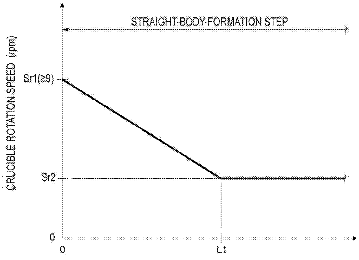
experiment 1
Between Rotation Speed of Crucible and Dislocation
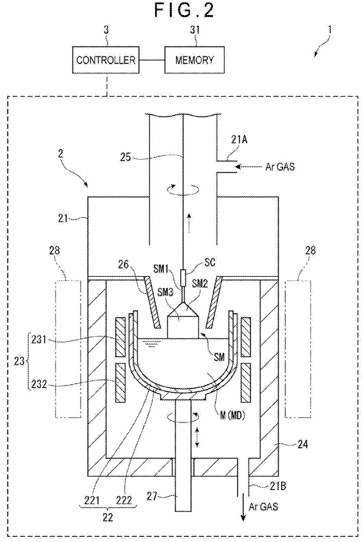
Manufacturing Method of Monocrystalline Silicon
experiment 2
Between Dislocation and Height of Remelt Growth Area
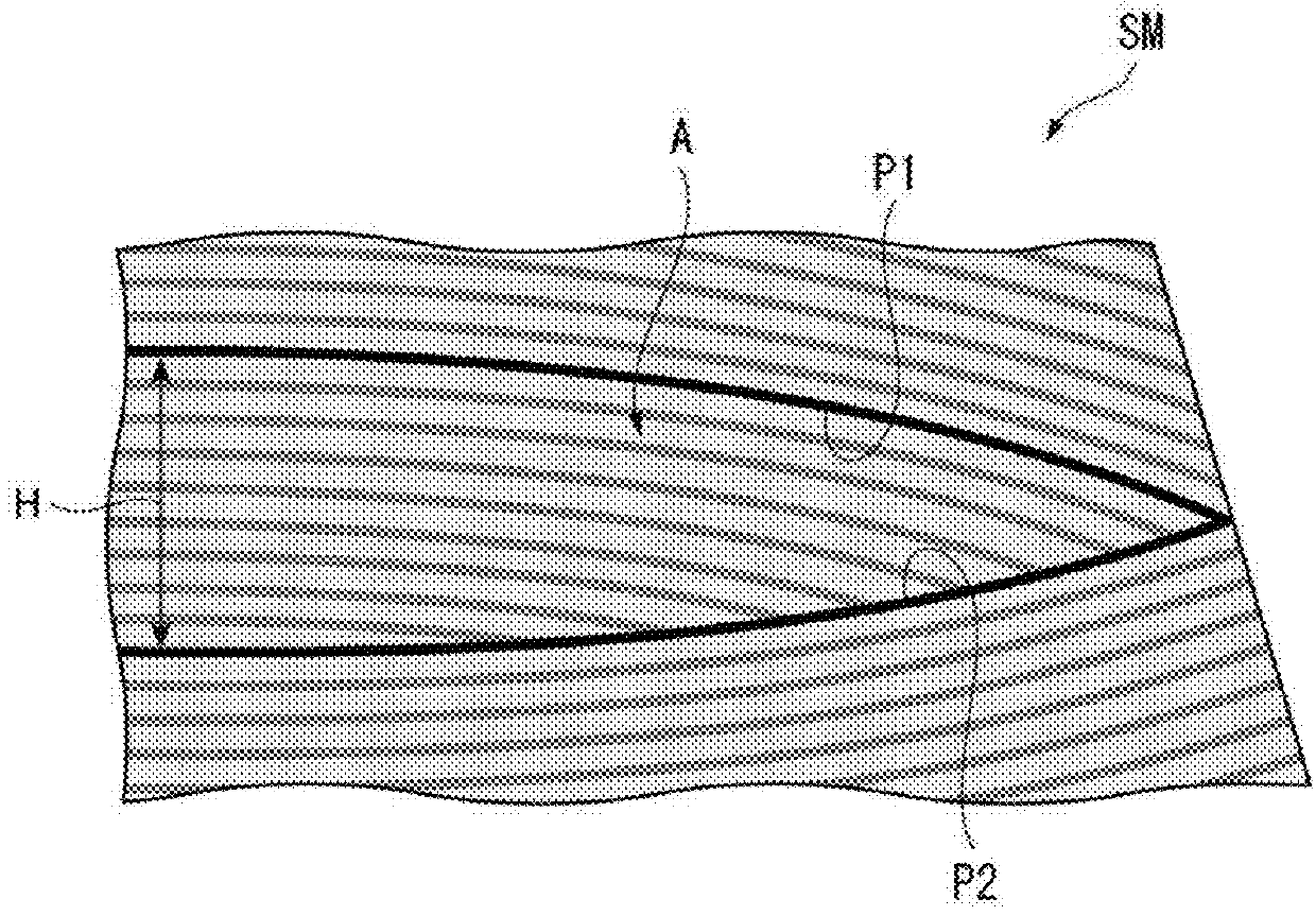
[0084]The monocrystalline silicons of Comparatives 1 and 3, in which dislocation occurred, were each vertically cut at a center in a radial direction, and the obtained cross section of the straight body was observed on X-rays to evaluate the number and the height of the remelt growth area(s). The same evaluation was also performed on the monocrystalline silicons of Examples 1, 2 and 6 in which no dislocation occurred. FIG. 5 shows the results of Comparative 1 and Examples 1 and 2 and FIG. 6 shows the results of Comparative 3 and Example 6.
[0085]As shown in FIGS. 5 and 6, the straight body of each of Examples 1, 2 and 6 had remelt growth areas of less than 200 μm in height but no remelt growth area of 200 μm or more. In contrast, the straight body of each of Comparatives 1 and 3 had not only remelt growth areas of less than 200 μm but also ones of 200 μm or more. Further, since no dislocation occurred in the monocrystalline silicons...
PUM
| Property | Measurement | Unit |
|---|---|---|
| height | aaaaa | aaaaa |
| diameter | aaaaa | aaaaa |
| electrical resistivity | aaaaa | aaaaa |
Abstract
Description
Claims
Application Information
 - R&D
- Intellectual Property
- Life Sciences
- Materials
- Tech Scout
- Unparalleled Data Quality
- Higher Quality Content
- 60% Fewer Hallucinations
Browse by: Latest US Patents, China's latest patents, Technical Efficacy Thesaurus, Application Domain, Technology Topic, Popular Technical Reports.
© 2025 PatSnap. All rights reserved.Legal|Privacy policy|Modern Slavery Act Transparency Statement|Sitemap|About US| Contact US: help@patsnap.com