Structure and method for forming strained finfet by cladding stressors

a technology of stressors and cladding, applied in the field of semiconductor devices, can solve the problems of device degradation and variation, strain relaxation (and strain loss) at the fin end, and achieve the effects of avoiding stress relaxation, preventing/recovering strain relaxation, and uniform stress

Active Publication Date: 2018-02-15
IBM CORP
View PDF6 Cites 4 Cited by
  • Summary
  • Abstract
  • Description
  • Claims
  • Application Information

AI Technical Summary

Benefits of technology

The present invention provides a method and structure for fabricating fins of FinFET devices that maintain uniform stress across the fin and prevent stress relaxation at the fin ends. The method involves using a cladding stressor material wrapped around the end of the fin to impose strain more efficiently and provide mechanical support to the fins. This results in a more effective strain and better mechanical performance of the fins. The invention also allows for the fabrication of SiGe fins and Si fins with different strain levels for NFET and PFET devices, respectively. The technical effects of the invention include improved performance and reliability of FinFET devices.

Problems solved by technology

However, when SiGe or Si fins are cut (e.g., etched) into desired lengths to meet the design requirements, strain relaxes (and strain loss occurs) at fin ends.
The loss of strain at SiGe or Si fin ends causes device degradation and variation.

Method used


Image

  • Structure and method for forming strained finfet by cladding stressors
  • Structure and method for forming strained finfet by cladding stressors
  • Structure and method for forming strained finfet by cladding stressors

Examples


Embodiment Construction

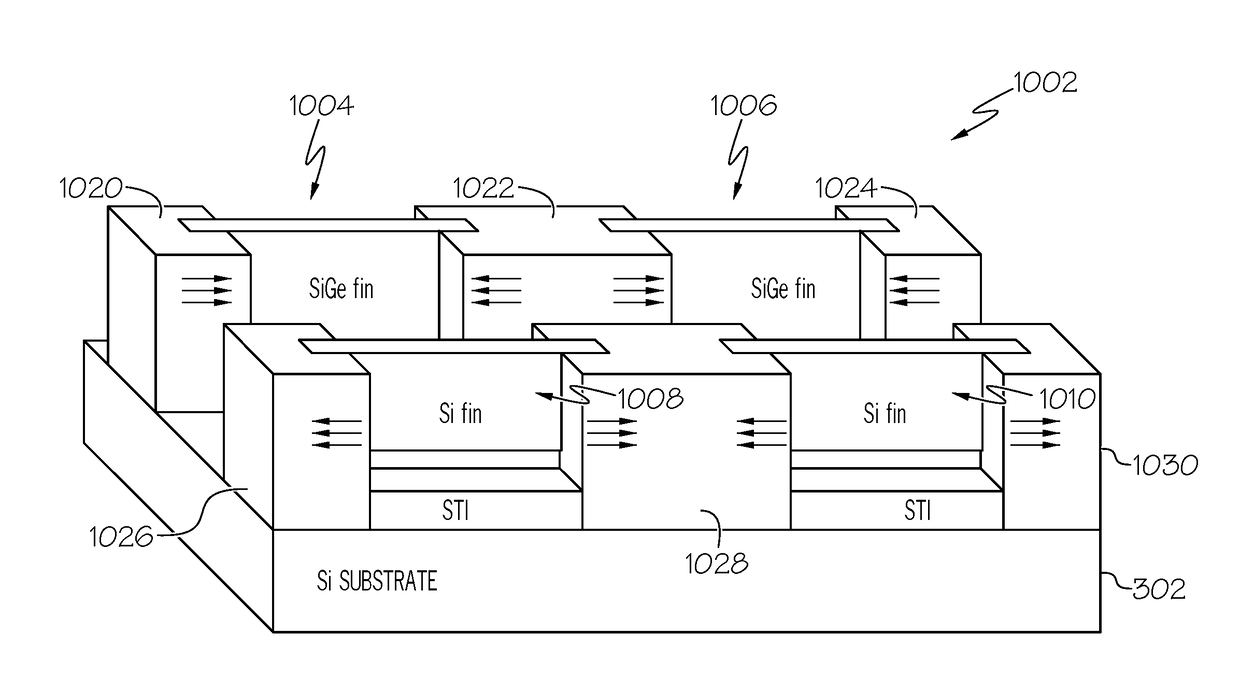
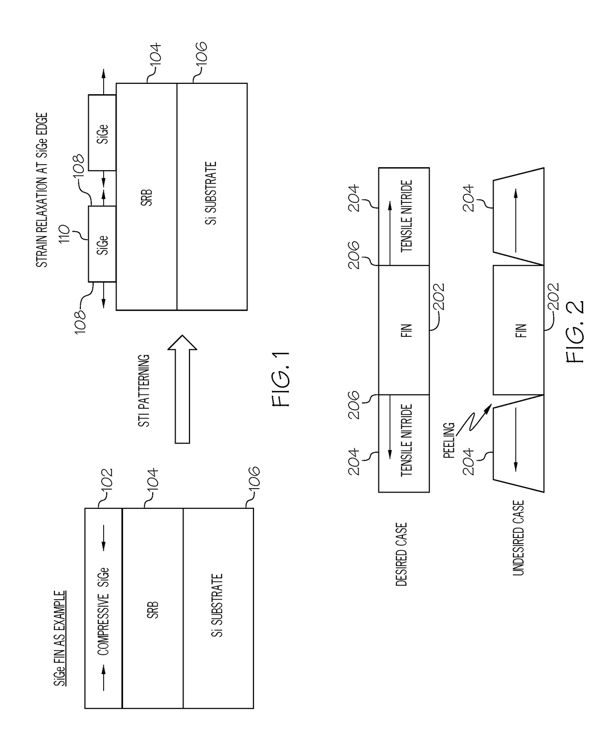
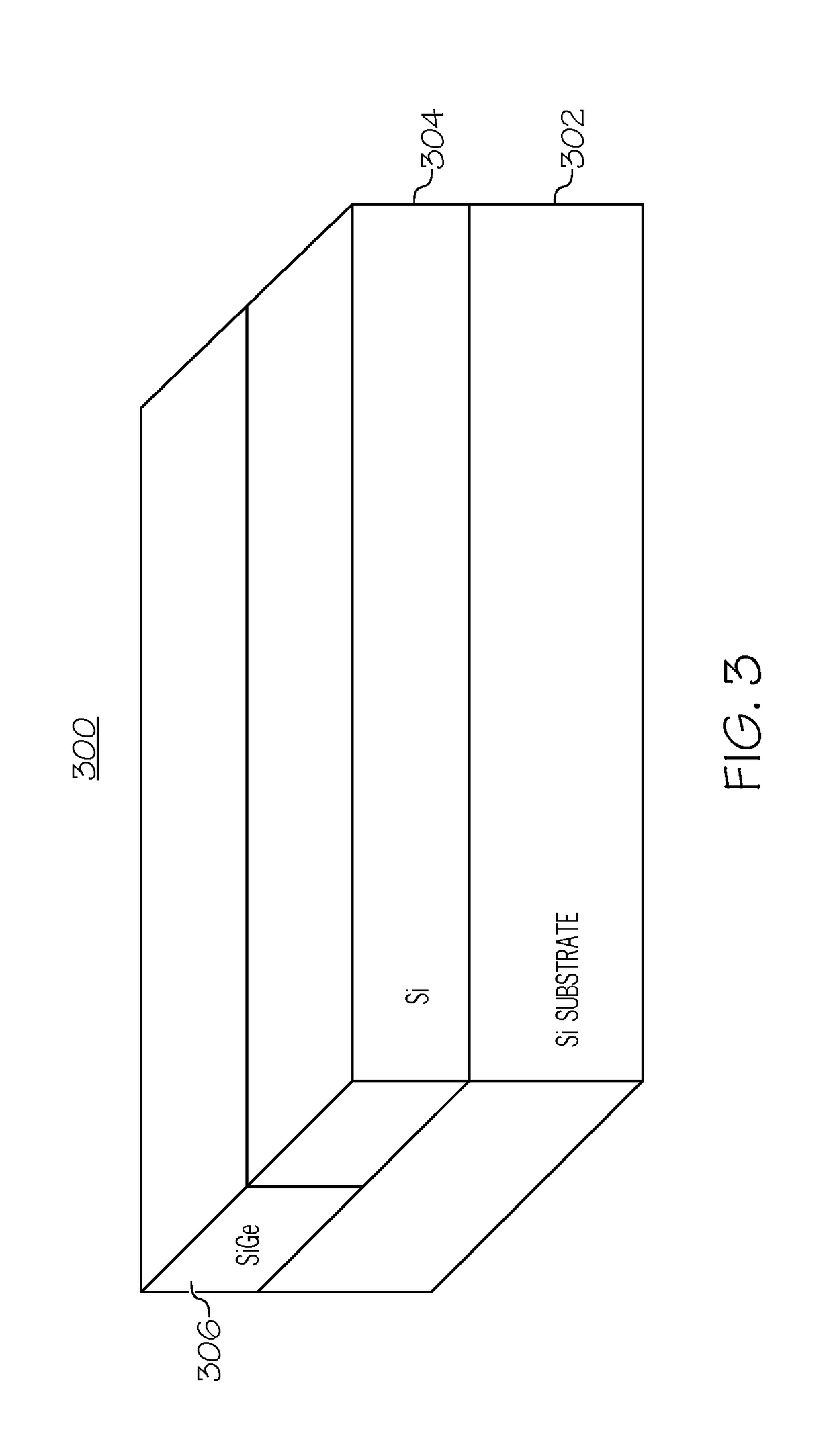
[0019]It is to be understood that the present invention will be described in terms of given illustrative example processes for fabricating strained FinFET devices. However, other semiconductor architectures, structures, substrate materials, and process features and steps may be varied within the scope of the present invention. The terms “strain”, “stress”, “strained”, and “stressed”, and the like, synonymously mean herein the same type of strain or stress that can be designed and fabricated in a fin semiconductor structure of a strained FinFET device.

[0020]It will also be understood that when an element such as a layer, region or substrate is referred to as being “on” or “over” another element, it can be directly on the other element or intervening elements may also be present. In contrast, when an element is referred to as being “directly on” or “directly over” another element, there are no intervening elements present. It will also be understood that when an element is referred to...


PUM


Abstract

Various methods and structures for fabricating a strained semiconductor fin of a FinFET device. A strained semiconductor fin structure includes a substrate, a semiconductor fin disposed on the substrate, the semiconductor fin having two fin ends, and a stressor material cladding wrapped around a portion of each of the two fin ends forming a strained semiconductor fin that includes at least one strained channel fin having stressor cladding wrapped around at least one end of the strained channel fin thereby straining the at least one strained channel fin. The stressor cladding can be a compressive nitride stressor to compressively strain a compressively strained silicon germanium fin. The stressor cladding can be a tensile nitride stressor to tensily strain a tensily strained silicon fin.

Description

BACKGROUND OF THE INVENTION[0001]The present invention generally relates to the field of semiconductors, and more particularly relates to a method of fabricating strained FinFET semiconductor devices.[0002]Strain engineering is highly desired for boosting CMOS performance Tensile strain is beneficial for nFET and compressive strain is beneficial for pFET.[0003]Strained high germanium percentage (Ge%) silicon germanium (SiGe) channel (compressive) and silicon (Si) channel (tensile) grown on strain relaxation buffer (SRB) substrate layer have been touted as a device option for continued scaling CMOS (complementary metal-oxide-semiconductor) technology beyond 7 nm node.[0004]However, when SiGe or Si fins are cut (e.g., etched) into desired lengths to meet the design requirements, strain relaxes (and strain loss occurs) at fin ends. The loss of strain at SiGe or Si fin ends causes device degradation and variation.[0005]Therefore, there is a need to fabricate SiGe fins and Si fins to pre...

Claims


Application Information

Patent Timeline
IPC IPC(8): H01L29/78H01L27/12H01L29/66H01L29/06H01L29/165
CPCH01L29/7848H01L29/785H01L27/1211H01L29/165H01L29/66795H01L29/0649H01L21/823821H01L21/845H01L29/7846H01L27/0924H01L21/823878
Inventor CHENG, KANGGUOLI, JUNTAO
Owner IBM CORP
Why Eureka
Try Eureka