
Polymer substrate for flexible electronics microfabrication and methods of use

a flexible electronics and microfabrication technology, applied in the direction of dielectric characteristics, organic semiconductor devices, dielectric components, etc., can solve the problems of inability to reliably and reproducibly align existing backplane substrates, the limit of flexible substrate materials seen today in the microfabrication of low-cost and high-yield flexible backplane tft stacks, and the inability to meet the requirements of microfabrication requirements. , to achieve the effect of improving performance,

Active Publication Date: 2017-11-23
ARES MATERIALS INC
View PDF2 Cites 18 Cited by
  • Summary
  • Abstract
  • Description
  • Claims
  • Application Information

AI Technical Summary

Benefits of technology

The patent text describes using a method called thiol-'click' reactions to create substrates that can stick to other materials like metals or metal oxides. By adding specific chemicals to the substrate, the surface can be made reactive and able to bond with these materials. This can be useful for creating electronic components that are more efficient, effective, or easier to make.

Problems solved by technology

A limitation seen today in the microfabrication of low-cost and high-yield flexible backplane TFT stacks is the flexible substrate material.
However, this method may lead to non-uniformity of the substrate surface due to the evaporation required for the solid fraction to precipitate and form a continuous film.
However, in these applications a substantial fraction may remain in the solid film after curing and this may cause off-gassing during sensitive processing applications such as high-vacuum deposition or thermal annealing.
Other challenges in flexible display backplane manufacturing may be due at least in part to the photolithographic processes that the substrate of the backplane must withstand.
Even at temperatures below second-order transition and phase-change temperatures, existing backplane substrates do not allow for reliable and reproducible alignment over subsequent photolithographic steps requiring thermal cycling or cycling of other environmental stimuli.
In addition, creep, fatigue, and micro-to-macro-scale network rearrangement cause problems for existing backplane substrates and render them inadequate at higher temperatures, such as those often required for formation of additional backplane structures on the substrate or further electronics structures on the backplane.
However, this interface is typically poor due to the lack of covalent or metallic bonding between the flexible and rigid components.
Additionally, mismatches in the physical properties of the materials such as the coefficient of thermal expansion (hereafter “CTE”) can lead to interfacial stresses which when coupled with a poor adhesion at the flexible-rigid interface, lead to delamination of the devices from the substrate and ultimately device failure.
Most polymer processing techniques yield substrates with unsuitable surface roughness (Ra>5 nm) due to either technique-induced roughness (e.g. molding, extruding, etc.) or the nature of the polymer backbone behavior (e.g. semi-crystalline, liquid crystalline, etc.) However, by utilizing monomeric or oligomeric precursor solutions, a film may be deposited via a plurality of methods (e.g. die coating, blade coating, dip coating, etc.) that produce continuous films with low surface roughness (Ra<5 nm) and cure the materials in this final, smooth-surface state.
Current flexible electronics backplane materials, such as biaxially-oriented polyethylene naphthalate, polycarbonate, and polyimides, suffer from the inability to align multiple masks over thermal cycling, which may limit processing temperatures, size, and / or complexity of electronic structures.

Method used


Image

  • Polymer substrate for flexible electronics microfabrication and methods of use
  • Polymer substrate for flexible electronics microfabrication and methods of use
  • Polymer substrate for flexible electronics microfabrication and methods of use

Examples


example 1

[0056]The following table illustrates some of the properties of an example flexible polymeric substrate film:

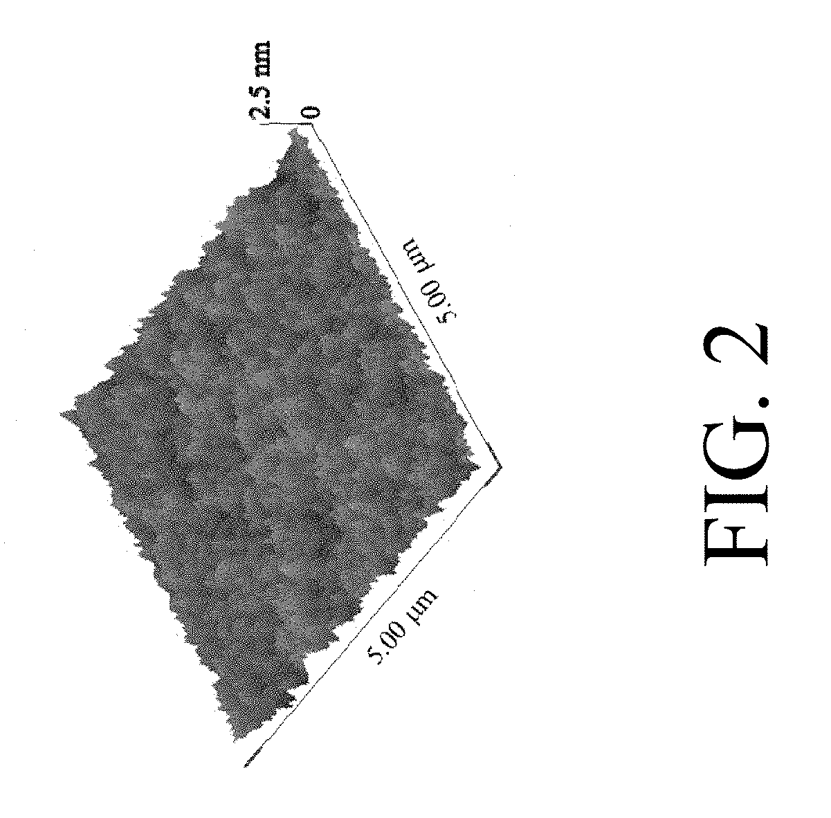
PropertyMeasurement RangeValueUnitsMethodPhysicalUltimate Tensile Strength25°C.55MPaASTM D170860°C.10100°C.3Ultimate Elongation25°C.5%ASTM D170860°C.135100°C.50Young's Modulus25°C.2GPaASTM D170860°C.0.1100°C.0.03ThermalCoefficient of Thermal Expansion0-50°C.35ppm / ° C.TMA(in-plane; linear)50-250°C.150Surface Roughness100μm2nmAFMGlass Transition (Tg)−40-200°C.53° C.DSCMelting Point (Tm)——° C.—Thermal Degradation - 1% (T1%)25-700°C.275° C.TGAThermal Degradation - 5% (T5%)25-700°C.360° C.TGAThermal Degradation - Onset (Td)25-700°C.370° C.TGAOpticalOptical Transmission230-375nm0-80 (linear)%UV-Vis365-450nm>80450-800nm>90Refractive Index—1.555—ASTM D542Retardation2000mm20.21nmASTM D4093Birefringence2000mm242nm / cmASTM D4093Haze2000mm20.46%ASTM D1003Chemical CompatibilityaPolar Protic Solvent (e.g. water)23°C.GOOD—Exp.Polar Aprotic Solvent (e.g. acetone)23°C.GOODb—Exp.Nonpolar Solven...

example 2

[0057]To a fluid reservoir was added the multifunctional thiol monomer trimethylolpropane tris(3-mercaptopropionate) (1 mol eq.) and the multifunctional co-monomer 1,3,5-Triallyl-1,3,5-triazine-2,4,6(1H,3H,5H)-trione (1 mol eq.), and the container was sealed. The sealed container was placed into a rotary mixer and mixed at 2350 rotations per minute (rpm) for 5 minutes. The container was removed from the mixer, opened, and 1.5 wt % of the free-radical initiator 2,2-dimethoxy-2-phenylacetophenone was added into the mixed monomer solution at room temperature (about 25° C.). The container was again sealed, placed into the rotary mixer and mixed at 2350 rpm for an additional 5 minutes. No organic solvent was added to the solution, resulting in the fluid reservoir containing a 100% (w / w) solid-fraction monomer solution. The monomer solution mixture was mounted to a slot-die coating tool and processed into a thin-film atop a carrier substrate via the slot-die coating technique. The cast mo...

example 3

[0059]A flexible polymeric substrate film was fabricated using a monomer solution of multifunctional thiol monomer Tri s[2-(3-mercaptopropionyloxy)ethyl] isocyanurate (1 mol eq.) and the multifunctional co-monomer Tris(4-hydroxyphenyl)methane triglycidyl ether (1 mol eq.). The monomer solution was placed in a sealed container. The sealed container was placed into a rotary mixer and mixed at 2350 rotations per minute (rpm) for 5 minutes. The container was removed from the mixer, opened, and 1.5 wt % of the catalyst tripropylamine was pipetted dropwise into the mixed monomer solution at room temperature (about 25° C.). The container was again sealed, placed into the rotary mixer and mixed at 2350 rpm for an additional 5 minutes. Finally, the container was again removed from the mixer, opened, and the organic solvent tetrahydrofuran was added until the final solution was a 92.5% (w / w) solute-fraction monomer solution. The monomer solution mixture was mounted to a slot-die coating tool ...


PUM


Abstract

Provided are flexible electronics stacks and methods of use. An example flexible electronics stack includes a flexible polymeric substrate film and a rigid inorganic electronic component. The flexible polymeric substrate film includes a thermoset polymer prepared by curing a monomer solution; wherein the monomer solution comprises about 25 wt % to about 65 wt % of one or more thiol monomers and from about 25 wt % to about 65 wt % of one or more co-monomers.

Description

BACKGROUND[0001]Substrate material choice for microfabrication is a factor used in the design of flexible electronics. Flexible displays are a type of flexible electronics. One of the core components in these devices is the display's backplane, which provides a matrix of addressable thin-film transistor (hereafter “TFT”) devices to control the display's pixels. The use of oxide-based semiconductors is becoming increasingly popular for large-area TFT fabrication. This is due to indium gallium zinc oxide (hereafter “IGZO”) TFTs' favorable electrical characteristics, and the ease of converting existing amorphous silicon manufacturing lines for compatibility with IGZO device fabrication. A limitation seen today in the microfabrication of low-cost and high-yield flexible backplane TFT stacks is the flexible substrate material.[0002]The fabrication of this substrate material is a critical step in order to enable these devices. Slot-die coating is a scalable manufacturing technique used to...

Claims


Application Information

Patent Timeline
IPC IPC(8): H01L27/12B05D3/00H01L29/786B05D1/00B05D1/28H05K1/18H01L27/32
CPCH01L27/1266B05D3/007B05D1/28B05D1/005H05K1/189H01L2227/326H01L27/1225H01L29/7869H01L2251/5338H01L27/3262H01L27/1218H01L29/78603H05K1/0393H05K2201/0108H10K77/111H10K59/1201H10K59/1213H10K71/80H10K2102/311
Inventor REIT, RADUAVENDANO-BOLIVAR, ADRIANARREAGA-SALAS, DAVID
Owner ARES MATERIALS INC
Learn More