
Optical transceiver by fowlp and dop multichip integration

a multi-chip integration and optical transceiver technology, applied in the field of compact optical transceivers, can solve the problems of serial link performance being limited by the electrical bandwidth of the channel and the electronic components, the inability to transfer photo, video, music, etc., and achieves the effect of low parasitic capacitance, low cost fowlp and tmv technology, and super-compact siz

Active Publication Date: 2017-09-07
MARVELL ASIA PTE LTD
View PDF0 Cites 23 Cited by
  • Summary
  • Abstract
  • Description
  • Claims
  • Application Information

AI Technical Summary

Benefits of technology

The present invention provides an improvement for packaging optical transceivers in a way that saves space and reduces parasitic capacitance. This is achieved by using a 3D die-on-package multichip stacking integration, which integrates photonics and electronics devices on separate chips. The use of lower cost technology and direct conductor ball bonding eliminates unreliable wire bonds and provides a more reliable assembly process. The invention also allows for flexible use of different electronic technologies for the driver / TIA and CDR or PAM4 ASIC, without the need for redesign of each chip. Overall, the invention improves the size and reliability of optical transceivers for broadband communication applications.

Problems solved by technology

But Internet and mobile applications continuously demand a huge amount of bandwidth for transferring photo, video, music, and other multimedia files.
Serial link performance is limited by the channel electrical bandwidth and the electronic components.
However, the process is very expensive and production yield is low due to the extreme complexity of the manufacturing process.
In system point of view, there is another drawback, i.e., wirebonding is still needed between electronic circuits and PCB or package substrate.
Therefore, there is no improvement in electrical signal transmission from PCB or package substrate to electronics circuits or vice versa.

Method used


Image

  • Optical transceiver by fowlp and dop multichip integration
  • Optical transceiver by fowlp and dop multichip integration
  • Optical transceiver by fowlp and dop multichip integration

Examples


Embodiment Construction

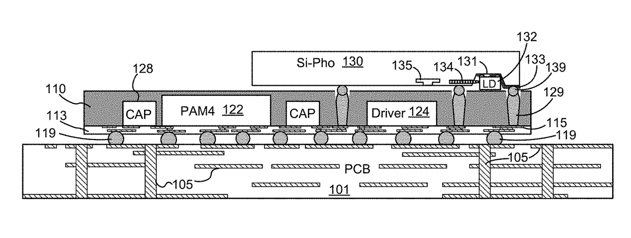
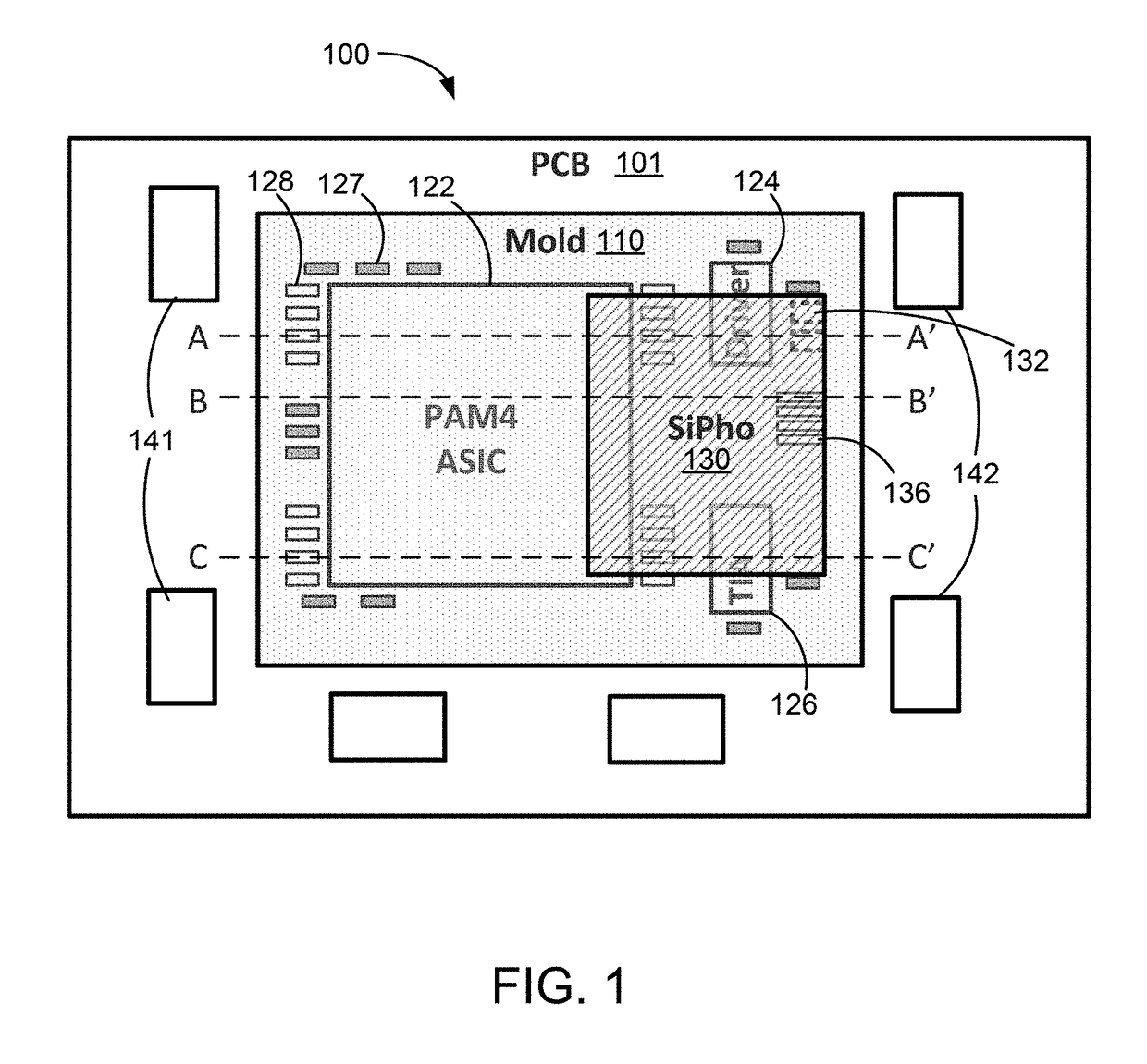
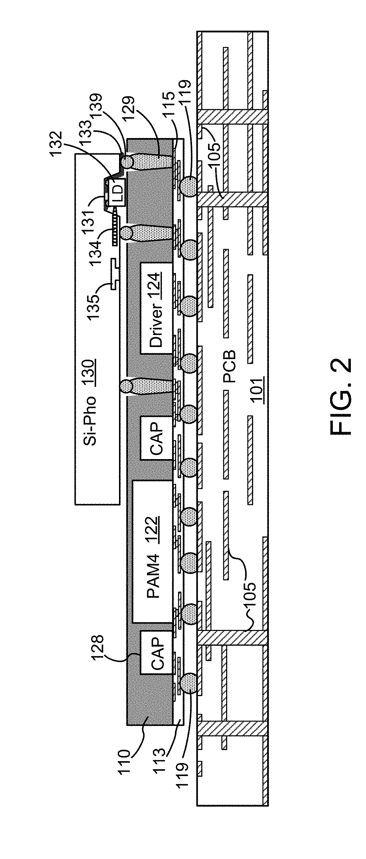
[0018]The present disclosure is related to an integrated photonics device. More particularly, a high-speed compact optical transceiver is formed by a die-on-package (DoP) multichip integration of a high-yield silicon photonics chip stacking over a FOWLP packaged electronics chip with through-mold vias (TMVs) for electrical coupling. In certain embodiments, the invention is applied for high speed optical communication, though other applications are possible.

[0019]The following description is presented to enable one of ordinary skill in the art to make and use the invention and to incorporate it in the context of particular applications. Various modifications, as well as a variety of uses in different applications will be readily apparent to those skilled in the art, and the general principles defined herein may be applied to a wide range of embodiments. Thus, the present invention is not intended to be limited to the embodiments presented, but is to be accorded the widest scope consi...


PUM


Abstract

An optical transceiver by hybrid multichip integration. The optical transceiver includes a PCB with a plurality of prefabricated surface bonding sites. A first chip includes a FOWLP package of multiple electronics devices embedded in a dielectric molding layer overlying a dielectric redistribution layer is disposed on the PCB by respectively bonding a plurality of conductor balls between the dielectric redistribution layer and the plurality of prefabricated surface bonding sites while exposing soldering material filled in multiple through-mold vias (TMVs) in the dielectric molding layer. The optical transceiver further includes a second chip configured as a Sipho die comprising photonics devices embedded in a SOI wafer substantially free from any electronics device process. The second chip is stacked over the first chip with multiple conductor bumps being bonded respectively to the soldering material in the multiple TMVs.

Description

CROSS-REFERENCE TO RELATED APPLICATIONS[0001]N / ABACKGROUND OF THE INVENTION[0002]The present disclosure is related to an opto-electrical integration, more particularly, to a compact optical transceiver based on Die-on-Package multichip stacking integration utilizing low cost Fan-Out Wafer Level Packaging (FOWLP) architecture and through-mold via (TMV) technology.[0003]As science and technology are updated rapidly, processing speed and capacity of the computer increase correspondingly. The communication transmission or reception using the traditional cable is limited to bandwidth and transmission speed of the traditional cable and mass information transmission required in modern life causes the traditional communication transmission overload. To correspond to such requirement, the optical fiber transmission system replaces the traditional communication transmission system gradually. The optical fiber communication is chosen for systems requiring higher bandwidth and longer distance t...

Claims


Application Information

Patent Timeline
Patent Type & Authority Applications(United States)
IPC IPC(8): G02B6/42G02B6/13H01L25/16H01L21/768H01L21/56G02B6/30H01L23/00
CPCG02B6/428H01L2924/10253G02B6/4295G02B6/30G02B6/13G02B6/4283H01L24/11H01L24/81H01L21/76877H01L21/565H01L25/167G02B2006/12142G02B2006/12121H01L2224/11334H01L2224/12105H01L2224/13014H01L2224/13016H01L2224/16227H01L2224/81191H01L2224/16146H01L2924/06H01L2924/1433H01L2924/1426H01L2924/141H01L2924/1205H01L2924/12043H01L2924/12042G02B6/4232G02B6/424G02B6/4245H01L2924/19105H01L24/20H01L24/19H01L2224/16235H01L2224/81801H01L2224/13101H01L24/13H01L24/16H01L2924/014H01L2924/00014H01L2224/18H01L23/48
Inventor DING, LIANGNAGARAJAN, RADHAKRISHNAN L.COCCIOLI, ROBERTO
Owner MARVELL ASIA PTE LTD
Learn More