Method for forming silicon nitride film selectively on sidewalls or flat surfaces of trenches

Active Publication Date: 2017-08-31
ASM IP HLDG BV
View PDF5 Cites 293 Cited by
  • Summary
  • Abstract
  • Description
  • Claims
  • Application Information

AI Technical Summary

Benefits of technology

The patent discusses techniques for controlling the properties of a silicon nitride film deposited using plasma-enhanced chemical vapor deposition or atomic layer deposition. The film can be treated to have directionality of properties, which can improve its quality and stability. By controlling the intensity and direction of ion bombardment during deposition or treatment, the film can be made denser and have better mechanical properties. This is achieved using a plasma generated using a parallel plate electrode configuration. The directionality of film properties can be controlled by adjusting the plasma configuration, dose, and energy of ions. Overall, the patent provides techniques for controlling the quality and stability of silicon nitride films, which can be useful in various applications.

Problems solved by technology
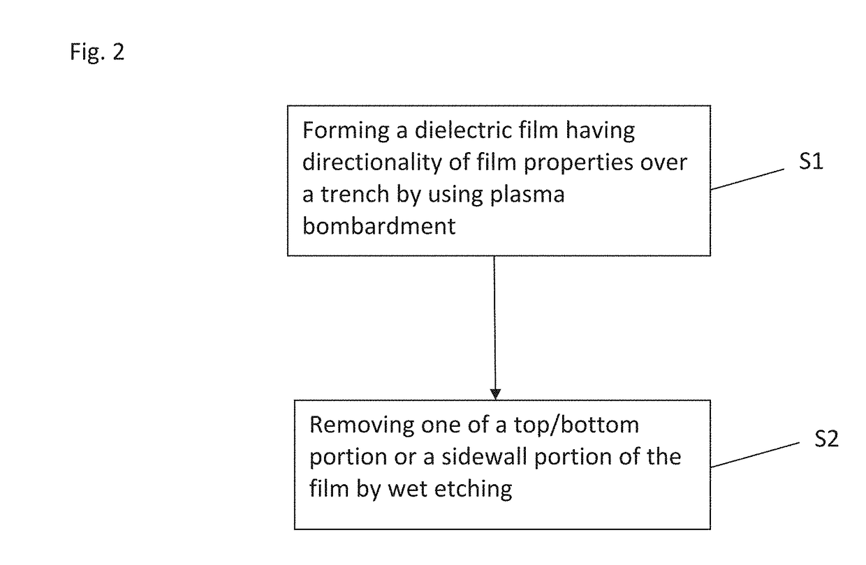
However, when such a formation method is used, over-etching is required in order to remove footing of sidewalls in which the thickness of the sidewalls increases near and at the bottom, forming a slope.
Over-etching causes etching of an underlying layer and causes damage to a layer structure.
That is, when ion bombardment is exerted on a silicon nitride film during deposition of the film or after the deposition of the film, impurities can be removed from the film, thereby causing densification of the film and improving the film quality; however, when ion bombardment is intensified and asymmetrically exerted on the dielectric film in a direction perpendicular to the film, the film quality is degraded, thereby dissociating Si—N bonds, decreasing the density of the film, and increasing wet etching rates.

Method used


Image

  • Method for forming silicon nitride film selectively on sidewalls or flat surfaces of trenches
  • Method for forming silicon nitride film selectively on sidewalls or flat surfaces of trenches
  • Method for forming silicon nitride film selectively on sidewalls or flat surfaces of trenches

Examples


example 1

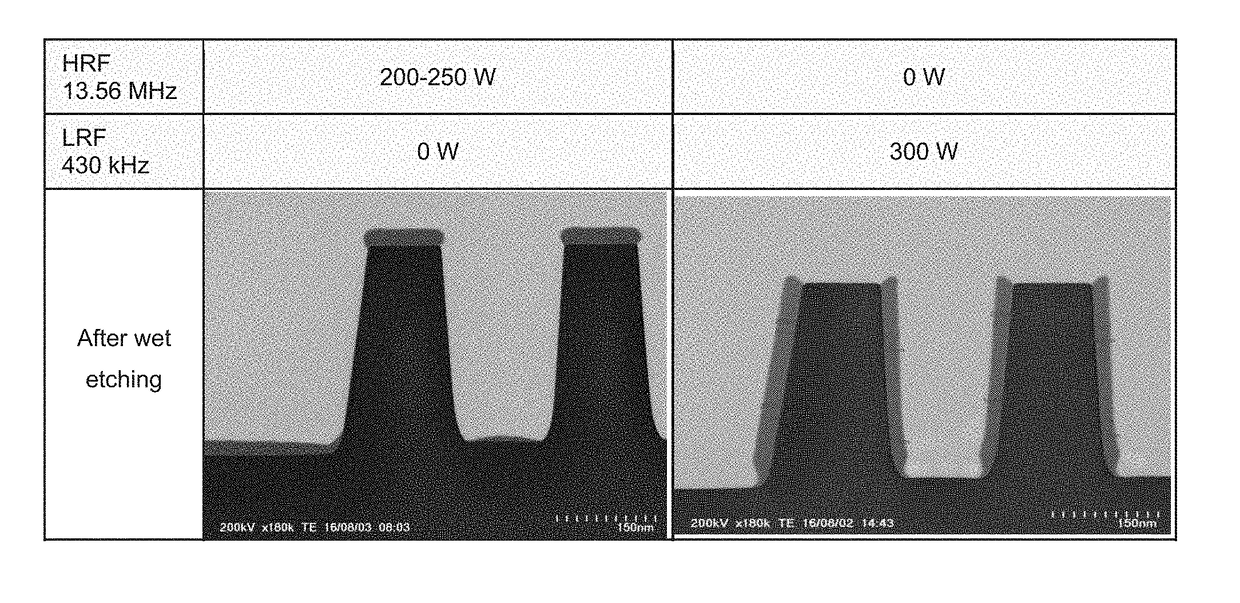
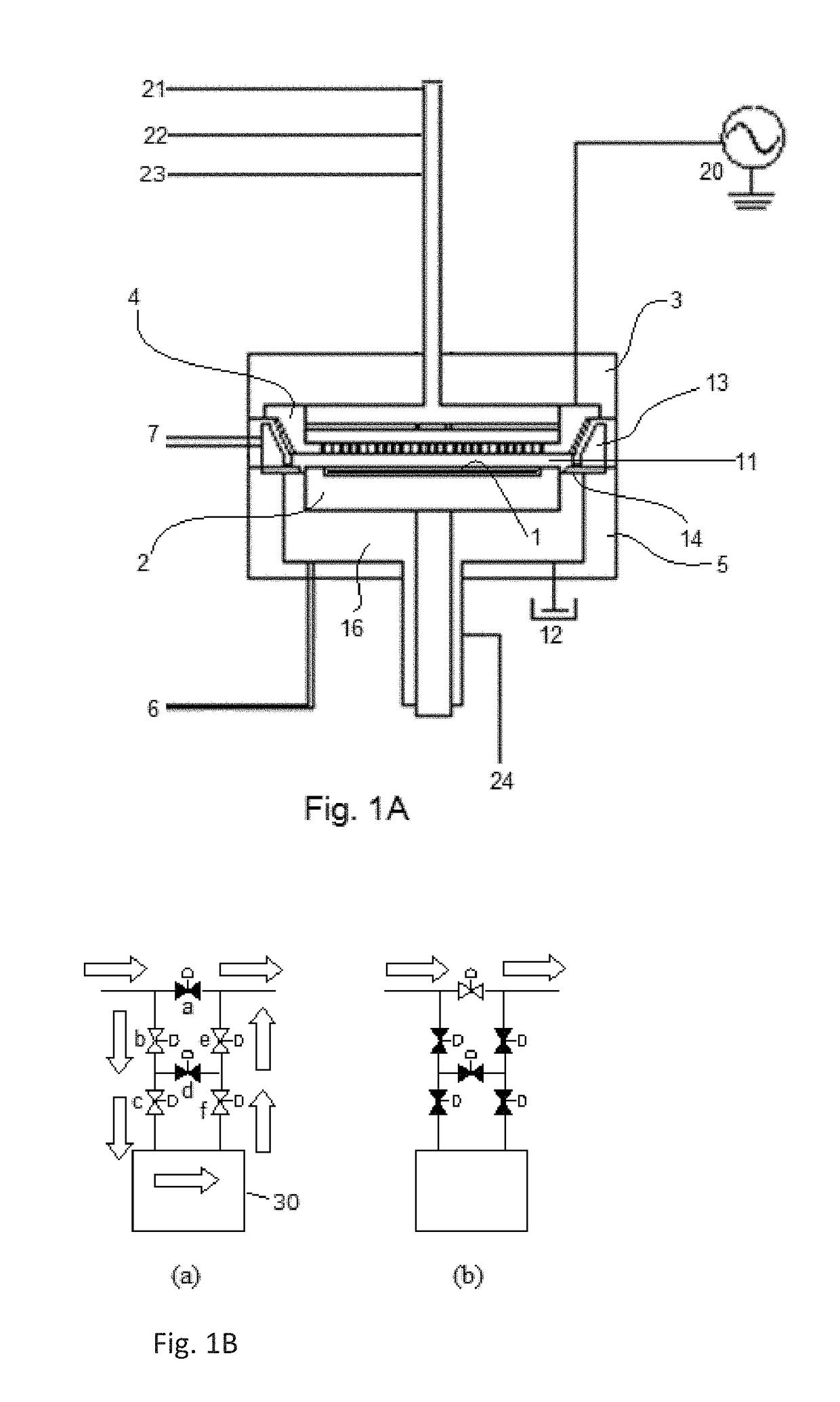
[0090]A SiN film was formed on a Si substrate (0300 mm) having trenches by PEALD, one cycle of which was conducted under the conditions shown in Table 4 (deposition cycle) below using the PEALD apparatus illustrated in FIG. 1A and a gas supply system (FPS) illustrated in FIG. 1B.

[0091]After taking out the substrate from the reaction chamber, the substrate was subjected to wet etching under the conditions shown in Table 4 below.

TABLE 4Conditions for Deposition CycleSubstrate temperature400°C.Pressure350 PaPrecursorSiI2H2Precursor pulse0.3 secPrecursor purge0.5 secReactantN2Flow rate of reactant2000 sccm(continuous)Flow rate of carrier 2000 sccm N2gas (continuous)Flow rate of dilution 0 sccmgas (continuous)RF power (13.56 MHz) Variable for a 300-mm wafer(see FIG. 7)RF power pulse3.3 secPurge0.1 secGrowth rate per cycle 0.05nm / cycle(on top surface)Number of cycles 200 times (10 nm)(thickness of film on top surface)Step coverage (side / top; 100%; 100%side / bottom)Trench depth / width (nm)10...

example 2

[0094]The SiN films were deposited under the conditions shown in Table 5, where the threshold RF power was determined to be approximately 400 W in the same manner as in Example 1. The SiN films were then subjected to wet etching under the conditions shown in Table 5. FIG. 8 shows Scanning Transmission Electron Microscope (STEM) photographs of cross-sectional views of the silicon nitride films. As can be seen from FIG. 8, when RF power was 700 W, the top / bottom portions of the film were selectively removed by wet etching, and substantially no film remained (no residual film was observed) on the top surface and at the bottom of the trench. When RF power was 500 W, the top / bottom portions of the film were more predominantly removed than was the sidewall portion of the film by wet etching, but residual film remained on the top surface and at the bottom of the trench, whereas the sidewall portion of the film mostly remained. When RF power was 300 W, the sidewall portion of the film was m...

example 3

[0095]The SiN film was deposited in the same manner as in Example 1 except that RF power was 880 W. The SiN film was then subjected to wet etching under the same conditions as in Example 1. FIG. 9 shows a Scanning Transmission Electron Microscope (STEM) photograph of a cross-sectional view of the SiN film after the wet etching. As can be seen from FIG. 9, substantially no film remained (no residual film was observed) on the top surface and at the bottom of the trench.


PUM


Abstract

A method for fabricating a layer structure in a trench includes: simultaneously forming a dielectric film containing a Si—N bond on an upper surface, and a bottom surface and sidewalls of the trench, wherein a top / bottom portion of the film formed on the upper surface and the bottom surface and a sidewall portion of the film formed on the sidewalls are given different chemical resistance properties by bombardment of a plasma excited by applying voltage between two electrodes between which the substrate is place in parallel to the two electrodes; and substantially removing either one of but not both of the top / bottom portion and the sidewall portion of the film by wet etching which removes the one of the top / bottom portion and the sidewall portion of the film more predominantly than the other according to the different chemical resistance properties.

Description

CROSS-REFERENCE TO RELATED APPLICATIONS[0001]This application is a continuation-in-part of U.S. patent application Ser. No. 15 / 048,422, filed Feb. 19, 2016, the disclosure of which is herein incorporated by reference in its entirety. The applicant / inventors herein explicitly rescind and retract any prior disclaimers or disavowals made in any parent, child or related prosecution history with regard to any subject matter supported by the present application.BACKGROUND[0002]Field of the Invention[0003]The present invention relates generally to a method for fabricating a layer structure constituted by a dielectric film containing a Si—N bond in a trench formed in an upper surface of a substrate.[0004]Related Art[0005]In manufacturing processes of large-scale integrated circuits (LSIs), there are several processes for forming sidewalls in trenches. The sidewalls are used as spacers or used for blocking etching of a structure from side surfaces of trenches. Conventionally, the sidewalls w...

Claims


Application Information

Patent Timeline
IPC IPC(8): H01L21/02H01L21/311
CPCH01L21/0217H01L21/0234H01L21/02274H01L21/0228H01L21/02211H01L21/31111H01J2237/3347
Inventor ISHIKAWA, DAIFUKAZAWA, ATSUKISHIBA, EIICHIROUEDA, SHINYAEBISUDANI, TAISHICHUN, SEUNGJUYOO, YONGMINMIN, YOONKIKIM, SEYONGCHOI, JONGWAN
Owner ASM IP HLDG BV
Why Eureka
Try Eureka